Semiconductor device with p-type AlxInyGal-x-yN and ohmic electrode thereof
a technology of ohmic electrodes and semiconductor devices, which is applied in the direction of semiconductor devices, electrical devices, transistors, etc., can solve the problems of increasing the amount of gate leakage current in the semiconductor device, and achieve the effect of reducing the amount of gate leakage current and fast switching characteristics
- Summary
- Abstract
- Description
- Claims
- Application Information
AI Technical Summary
Benefits of technology
Problems solved by technology
Method used
Image
Examples
embodiment 1
(Embodiment 1)
[0073]The following describes Embodiment 1 with reference to the drawings.
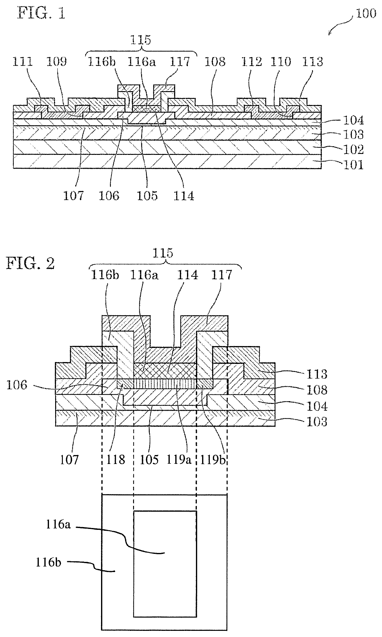
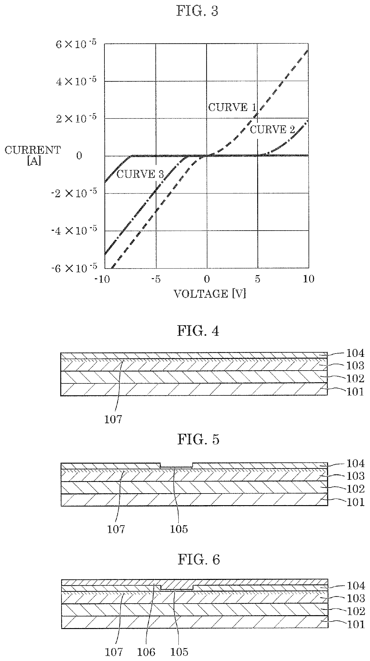
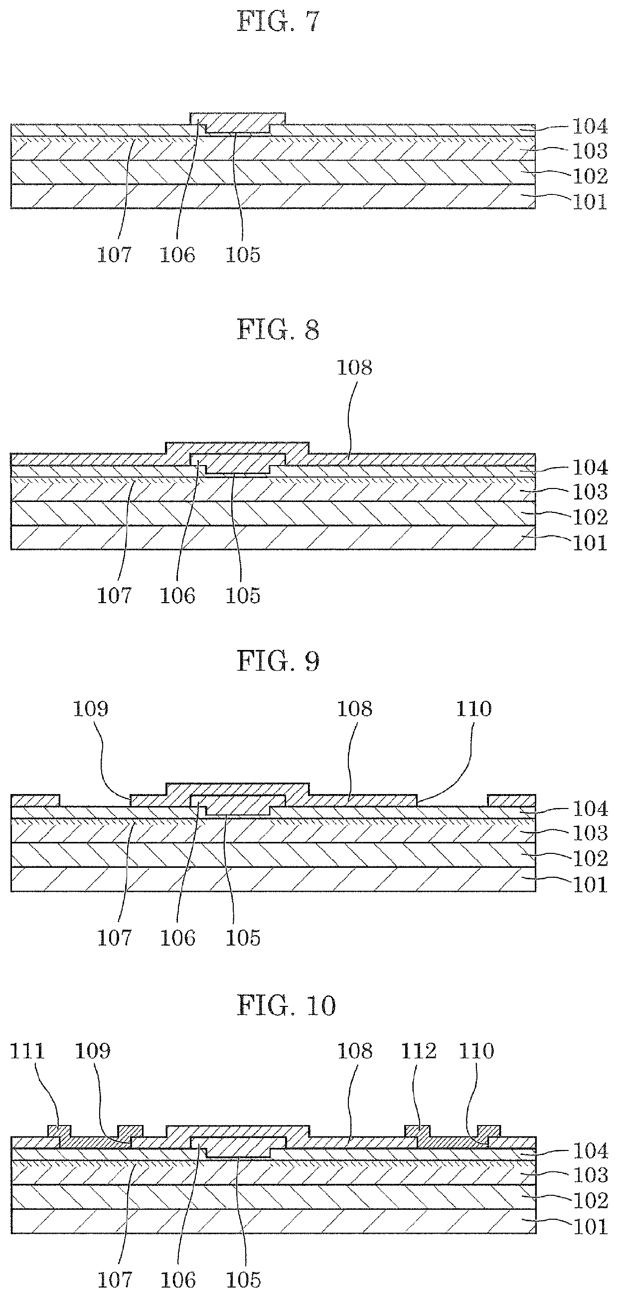
[0074]FIG. 1 is a cross-sectional view showing the structure of semiconductor device 100 according to the present embodiment. As shown in FIG. 1, semiconductor device 100 includes, for example, the following layers above substrate 101 that includes, for example, Si: buffer layer 102, with a thickness of 2 μm, having a multilayered structure including AlN and AlGaN; undoped (i-type) GaN layer 103 with a thickness of 2 μm; and i-type Al GaN layer 104 with a thickness of 80 nm and with an Al composition ratio of 15%. Note that “undoped (i-type)” means here that no impurity is intentionally doped in epitaxial growth. Also note that i-type AlGaN layer 104 corresponds to the semiconductor layer in the present disclosure.
[0075]Semiconductor device 100 includes, on a surface of i-type AlGaN layer 104, gate recess 105, with a depth of 60 nm, that has been processed into a predetermined shape. Semiconducto...
embodiment 2
(Embodiment 2)
[0106]The following describes Embodiment 2 with reference to the drawings. FIG. 15 is a cross-sectional view showing the structure of semiconductor device 200 according to the present embodiment. In FIG. 15, the same structural components as those shown in FIG. 1 are assigned with the same reference marks, and will not be described below.
[0107]Semiconductor device 200 according to Embodiment 2 is different from semiconductor device 100 according to Embodiment 1 in the structure of the gate electrode. More specifically, gate electrode 115 according to Embodiment 1 is partially in contact, via gate opening 114, with the surface of p-type GaN layer 106 that is opposite to the surface on which gate recess 105 is formed. Meanwhile, gate electrode 120 according to Embodiment 2 is entirely in contact with the surface of p-type GaN layer 106 that is opposite to the surface on which gate recess 105 is formed. Moreover, p-type GaN layer 106 and gate electrode 120 are processed i...
embodiment 3
(Embodiment 3)
[0127]The following describes Embodiment 3 with reference to the drawings. FIG. 26 and FIG. 27 are cross-sectional views showing the structure of semiconductor device 300 according to Embodiment 3. In FIG. 26 and FIG. 27, the same structural components as those shown in FIG. 1 are assigned with the same reference marks, and will not be described below.
[0128]Semiconductor device 300 according to Embodiment 3 is different from semiconductor device 100 according to Embodiment 1 in that semiconductor device 300 includes no gate recess 105 in a surface of i-type AlGaN layer 104.
[0129]In the case of semiconductor device 200 according to Embodiment 2, Ti film 121 is formed on a surface of p-type GaN layer 106, after which Ti film 121 and p-type GaN layer 106 are processed into the same shape. This results in an end face of p-type GaN layer 106 and an end face of Ti film 121 coming in contact with each other. Even in the case where the formation of gate recess 105 is omitted a...
PUM
| Property | Measurement | Unit |
|---|---|---|
| thickness | aaaaa | aaaaa |
| thickness | aaaaa | aaaaa |
| depth | aaaaa | aaaaa |
Abstract
Description
Claims
Application Information
 - R&D
- Intellectual Property
- Life Sciences
- Materials
- Tech Scout
- Unparalleled Data Quality
- Higher Quality Content
- 60% Fewer Hallucinations
Browse by: Latest US Patents, China's latest patents, Technical Efficacy Thesaurus, Application Domain, Technology Topic, Popular Technical Reports.
© 2025 PatSnap. All rights reserved.Legal|Privacy policy|Modern Slavery Act Transparency Statement|Sitemap|About US| Contact US: help@patsnap.com


