Organic electroluminescent device comprising delayed fluorescent materials
a technology of delayed fluorescent materials and electroluminescent devices, which is applied in the direction of basic electric elements, semiconductor devices, electrical equipment, etc., to achieve the effects of improving color tone, large degree of design freedom, and light emission efficiency of light having a short wavelength
- Summary
- Abstract
- Description
- Claims
- Application Information
AI Technical Summary
Benefits of technology
Problems solved by technology
Method used
Image
Examples
example 1
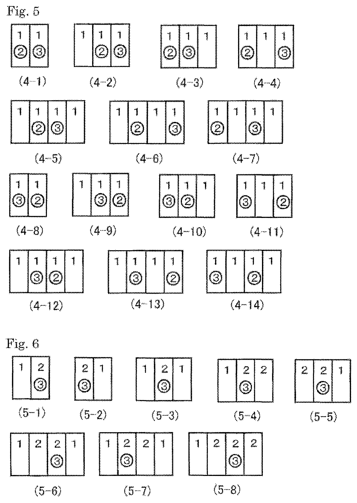
[0243]In this example, a multiple wavelength light emitting organic, electroluminescent device containing light emitting materials of three colors, i.e., a blue light emitting material, a green light emitting material and a red light emitting material, that were mixed in one light emitting layer was produced and evaluated.
[0244]Thin films were laminated on a glass substrate having formed thereon an anode formed of indium tin oxide (ITO) having a thickness of 100 nm, by a vacuum vapor deposition method at a vacuum degree of 5×10⁻⁴ Pa or less. Firstly, α-NPD was formed to a thickness of 35 nm on ITO, and thereon mCBP was formed to a thickness of 10 nm. ZHS02 as a blue light emitting material, 4CzIPN as a green light emitting material and 4CzTPN-Ph as a red light emitting material were vapor-co-deposited from separate vapor deposition sources to form a layer having a thickness of 15 nm, which was designated as a light emitting layer. At this time, the concentrations of 4CzIPN and 4CzTP...
examples 2 to 4
[0246]In these examples, multiple wavelength light emitting organic electroluminescent devices each containing light emitting materials of two colors, i.e., a blue light emitting material and a red light emitting material, that were mixed in one light emitting layer at three different concentrations were produced and evaluated.
[0247]Thin films were laminated on a glass substrate having formed thereon an anode formed of indium tin oxide (ITO) having a thickness of 100 nm, by a vacuum vapor deposition method at a vacuum degree of 5×10⁻⁴ Pa or less. Firstly, α-NPD was formed to a thickness of 35 nm on ITO, and thereon mCBP was formed to a thickness of 10 nm. 2CzPN as a blue light emitting material and 4CzTPN-Ph as a red light emitting material were vapor-co-deposited from separate vapor deposition sources to form a layer having a thickness of 15 nm, which was designated as a light emitting layer. At this time, the concentration of 4CzTPS-Ph was 0.1% by weight (Example 2), 0.2% by weigh...
example 5
[0249]In this example, a multiple wavelength, light emitting organic electroluminescent device having a light emitting layer containing a blue light emitting material doped with a red light emitting material that was held between light emitting layers each formed only of a blue light emitting material was produced and evaluated.
[0250]Thin films were laminated on a glass substrate having formed thereon an anode formed of indium tin oxide (ITO) having a thickness of 100 nm, by a vacuum vapor deposition method at a vacuum degree of 5×10⁻⁴ Pa or less. Firstly, α-NPD was formed to a thickness of 35 nm on ITO, then mCBP was formed thereon to a thickness of 10 nm, and ZHS02 as a blue light emitting material was formed to a thickness of 7 nm. ZHS02 and 4CzTPN-Ph as a red light emitting material were vapor-co-deposited from separate vapor deposition sources to form a layer having a thickness of 1 nm, which was designated as a light emitting layer. At this time, the concentration of 4CzTPN-Ph...
PUM
| Property | Measurement | Unit |
|---|---|---|
| energy difference | aaaaa | aaaaa |
| fluorescent | aaaaa | aaaaa |
| wavelength | aaaaa | aaaaa |
Abstract
Description
Claims
Application Information
 - R&D
- Intellectual Property
- Life Sciences
- Materials
- Tech Scout
- Unparalleled Data Quality
- Higher Quality Content
- 60% Fewer Hallucinations
Browse by: Latest US Patents, China's latest patents, Technical Efficacy Thesaurus, Application Domain, Technology Topic, Popular Technical Reports.
© 2025 PatSnap. All rights reserved.Legal|Privacy policy|Modern Slavery Act Transparency Statement|Sitemap|About US| Contact US: help@patsnap.com


