Medium wave infrared (MWIR) and long wavelength infrared (LWIR) operating microbolometer with raised strut design

a microbolometer and long-wavelength infrared technology, applied in the direction of optical radiation measurement, instruments, semiconductor devices, etc., can solve the problems of a small group of low-cost, low-performance products, and the sensitivity and abilities of these quantum detectors far surpass thermal detectors, so as to minimize the thermal conductance of the device , the effect of allowing

Active Publication Date: 2019-11-19
DELAWARE STATE UNIV FOUND INC
View PDF12 Cites 0 Cited by
  • Summary
  • Abstract
  • Description
  • Claims
  • Application Information

AI Technical Summary

Benefits of technology

[0004]The microbolometer encompasses a change in resistance on the sensing material due to absorption of heat flux on the detector, causing a change across the sensing material's resistance to be measured across the electrodes. Using a cavity layer followed by a mesh support structure minimizes the thermal conductance of the device—allowing the effective thermal conductance to be governed by the radiation over the detector.
[0009]The invention has support layers which is comprised of two stages. The first is a bottom support structure, creating the outer walls of the cavity which touches the substrate. The second is the mesh structure, creating an air cavity and minimizing the thermal conductance of the device struts to transfer heat away from the sensing layer to the substrate. Both support structures will be fabricated using e-beam lithography. The lower support layer is formed on top of the insulating layer by electron beam lithography while the upper support layer is fabricated by electron beam lithography on top of the lower support layer, and forming the lower cavity between the upper support layer and the insulating layer. The lower support layer and the upper support layers are made of insulating material having low thermal conductance, and transmittance of the lower support layer and the upper support layer is at least 60% between the wavelength ranges 0.2 μm to 7 μm. The upper support layer is on the lower support layer above an air cavity and is made of Al2O3, SiN or an insulating material. The upper support layer is a mesh like design structure made of Al2O3, SiN or an insulating material. The upper support layer has a thickness of 1 μm and a critical dimension between 60 nm and 120 nm and includes about 50 to 100 struts to minimize thermal conductance of the device below 5×10⁻⁹ W / K. The microbolometer lower support layer has a thickness of 2 μm and a critical dimension between 60 nm and 120 nm.
[0013]Top electrode has the same critical dimension as the supporting layer of 100 nm, and is meandered following the mesh structure, further reducing direct heat conduction from the sensing layer to the substrate. The electrodes are formed on top of the upper support layer using electron beam lithography, and positioned between the sensing layer and extending in a meandered shape, tracing the top support design to the ends of the detector design.
[0014]In a preferred embodiment, the semiconducting microbolometer has an absorption layer which has high absorption in MWIR and LWIR regions. The absorber layer of disk shape is positioned on top of the sensing layer. The absorber layer is made of NiCr or Au-black in a disk shape, with a thickness of about 0.2 μm and a diameter of 25 μm. The absorber layer is fabricated using photolithography with a sacrificial layer. The absorber layer provides a larger surface area than the sensing layer, providing a larger heat flux falling on the device.
[0017]The invention includes the approach of reducing the thermal conductance between the substrate and the sensing layer by reducing the thickness of the electrode layer and making the electrode layer shape meandered. Smaller thickness of metal electrode layer led to smaller cross-sectional area which provided a higher thermal resistance for conductive heat to flow. By changing the shape of the metal electrode layer meandered, the path length of the electrodes is increased for heat to conduct and thus the heat through these metal electrodes was reduced along with the supporting structure and contributed towards decrease in thermal conductance.
[0019]In this work, a thinner web structure was used which reduces the cross-sectional area of web structure and increases the thermal resistance of conductive heat flow. The decrease in thermal conductance was obtained by decreasing the thickness of the mesh structure. The decrease in thermal conductance was also obtained by decreasing the width of the strut.

Problems solved by technology

The sensitivity and abilities of these quantum detectors far surpassed thermal detectors, leaving them only useful for a small group of low-cost, low performance products.

Method used


Image

  • Medium wave infrared (MWIR) and long wavelength infrared (LWIR) operating microbolometer with raised strut design
  • Medium wave infrared (MWIR) and long wavelength infrared (LWIR) operating microbolometer with raised strut design
  • Medium wave infrared (MWIR) and long wavelength infrared (LWIR) operating microbolometer with raised strut design

Examples


Embodiment Construction

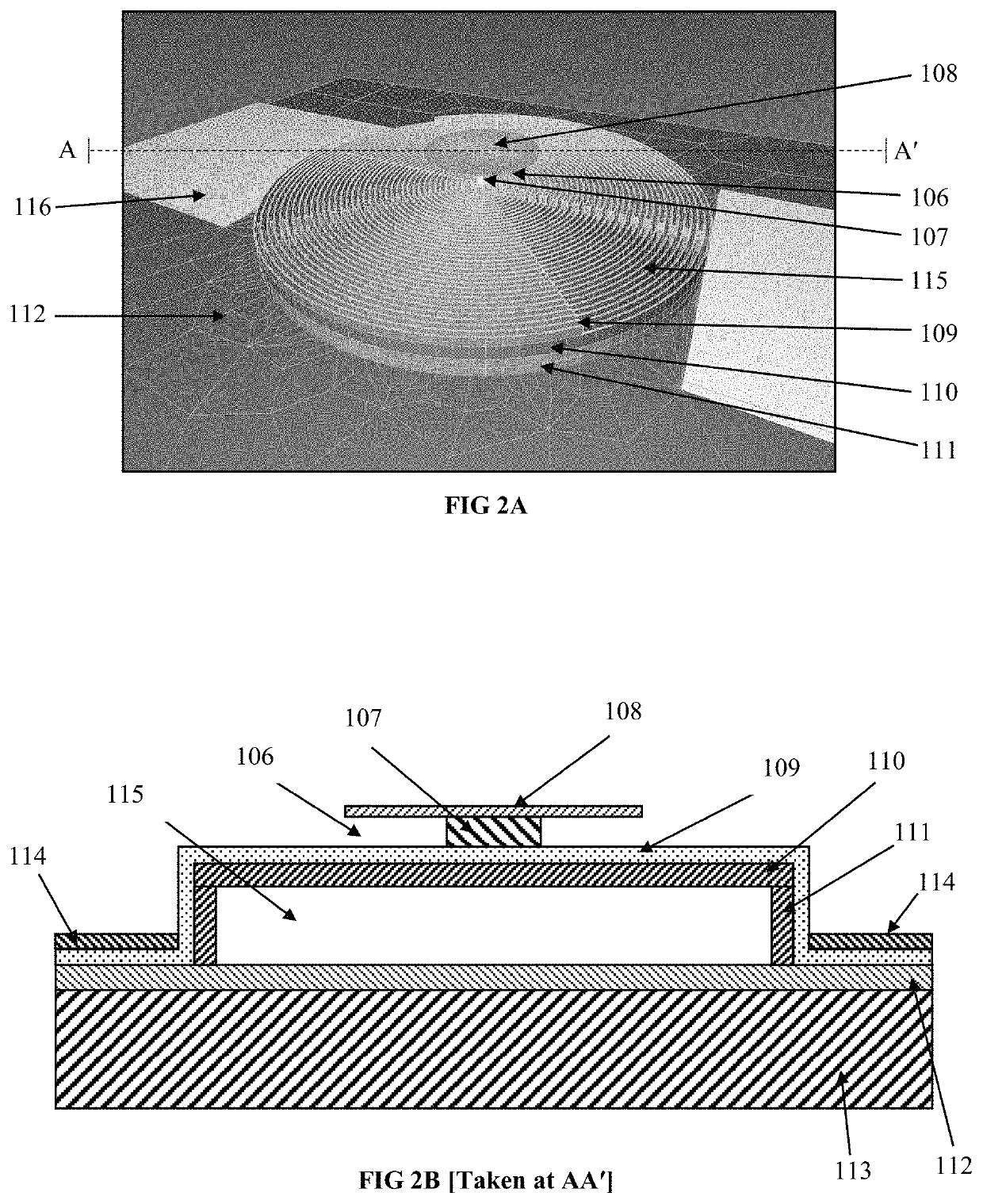
[0040]Various example embodiments will be described more fully hereinafter with reference to the accompanying drawings, in which some example embodiments are shown. Example embodiments may, however, be embodied in many different forms and should not be construed as limited to the example embodiments set forth herein. In the drawings, the sizes and relative sizes of layers and regions may be exaggerated for clarity.

[0041]In other example embodiments mentioned hereinafter describes some objects or layers as located above others, using terms such as “on top of” or “above”. Such example embodiments may be referring to any layer located above the first mentioned layer, but not necessarily the adjacent or closest layer to the original object. For example, a layer of material referred to as “above” another layer may be located directly above the original layer or several layers above the original layer.

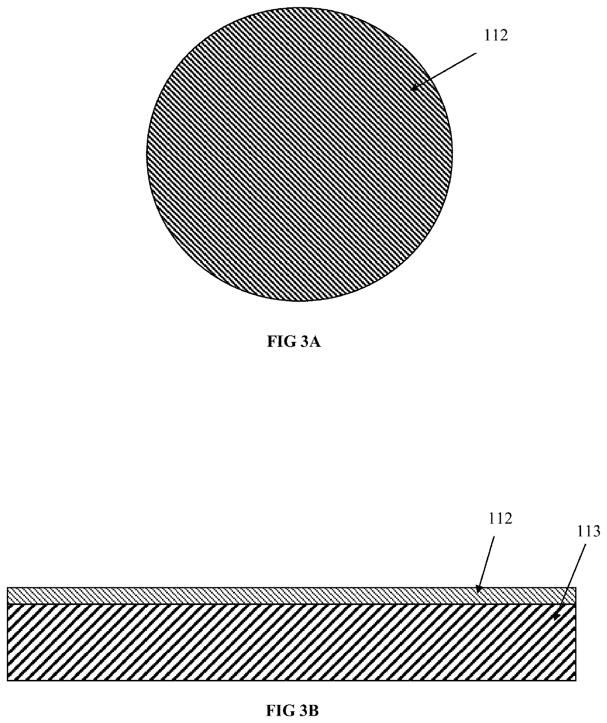
[0042]For microbolometers made of semiconducting sensing layers (semiconducting microbol...


PUM


Abstract

A semiconducting microbolometer sensor for detecting electromagnetic waves in the medium wavelength infrared (MWIR) and long-wavelength infrared (LWIR) is provided. A preferred embodiment provides a substrate layer, a bottom and top support structure with a strut-based mesh design, a meandered electrode layer that follows the top support structure design, a bolometer sensing material with a high TCR, and a disk-shaped absorber on top of the sensing material to maximize the heat flux absorption on the sensor. The bottom support of the sensor suspends the top support mesh, creating an air cavity. This air cavity along with the strut based mesh design and optimized thickness, dimension and shape of the layers contributed towards minimizing the thermal conductance of microbolometer and hence improved the figures of merits—responsivity, detectivity, noise equivalent power and noise equivalent temperature difference of microbolometer.

Description

TECHNICAL FIELD[0001]This invention reports the design and fabrication of a microbolometer which operates in MWIR (3 to 5 μm) and LWIR (8 to 14 μm) wavelengths for detecting infrared (IR) radiation. These types of IR detectors operate in room temperature without external or cryogenic cooling.BACKGROUND OF THE INVENTION[0002]Thermal IR detectors are heated by the incident IR radiation and provide detection through the change in a measurable parameter. They are used in contact-less temperature measurement, night vision cameras for defense, security and surveillance applications, search and rescue and many other thermal imaging applications. For these types of detectors, wavelengths of interest are mainly in the atmospheric windows—ranging from 3 to 5 (MWIR) and 8 to 14 (LWIR) μm wavelength ranges, due to the high transmission through atmospheric air of more than 80% and peak IR emission of room temperature bodies is at 9-10 μm of wavelengths. Until recently, the important market of th...

Claims


Application Information

Patent Timeline
Patent Type & Authority Patents(United States)
IPC IPC(8): H01L31/024G01J5/02H01L31/0352G01J5/20H01L31/18H01L31/09
CPCG01J5/20H01L31/18H01L31/09H01L31/0352H01L31/024G01J5/0225
Inventor RANA, MUKTIVOSHELL, ANDREW BODHI
Owner DELAWARE STATE UNIV FOUND INC
Why Eureka
Try Eureka