Chip resistor and method for producing chip resistor

a technology of resistors and chips, applied in the field of chip resistors, can solve the problems of resistor cutting by dicing, resistor details, and inability to recognize dicing positions,

Active Publication Date: 2019-09-10
KOA CORP
View PDF6 Cites 0 Cited by
  • Summary
  • Abstract
  • Description
  • Claims
  • Application Information

AI Technical Summary

Benefits of technology

[0014]According to the present invention, it is possible to realize a chip resistor which can prevent dicing failure of cutting a resistive element by mistake and which is suitable for bulk mounting.

Problems solved by technology

For this reason, when the front electrodes and the resistive elements are covered with the protective layer, dicing positions become unable to recognize.
In the worst case, a problem of cutting the resistive elements by dicing may arise.

Method used


Image

  • Chip resistor and method for producing chip resistor
  • Chip resistor and method for producing chip resistor
  • Chip resistor and method for producing chip resistor

Examples


Embodiment Construction

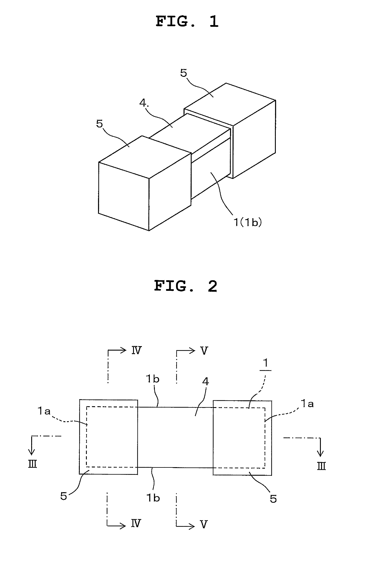
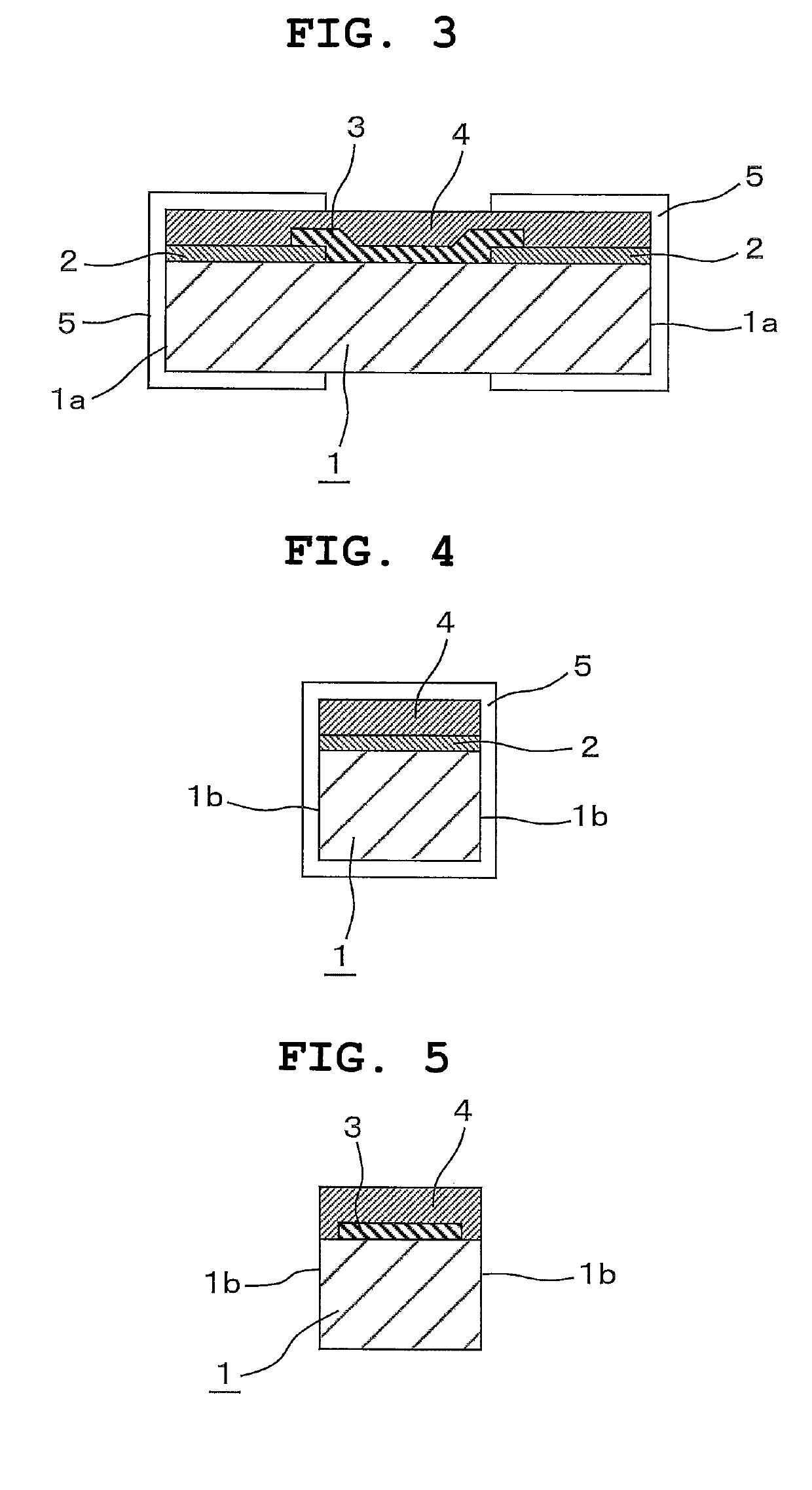
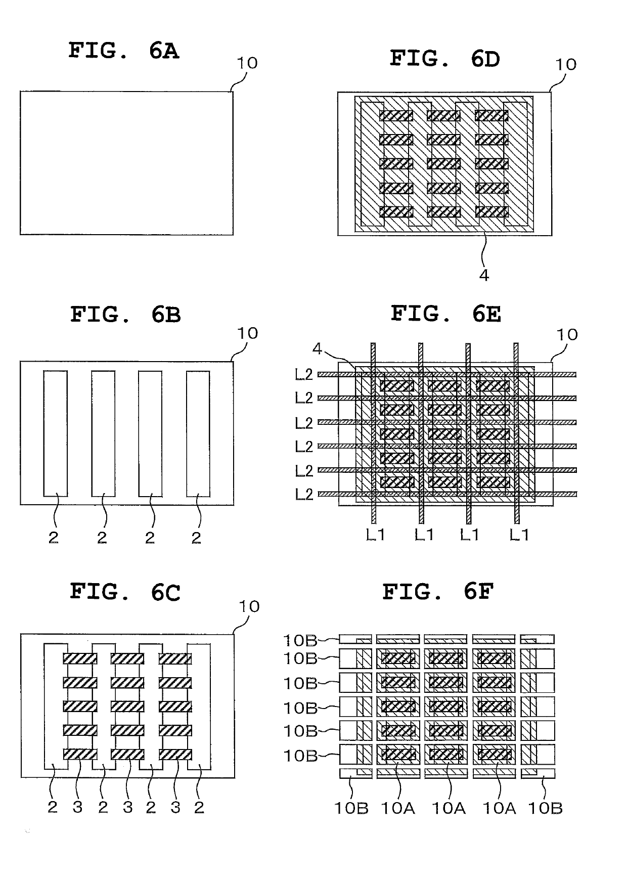
[0022]A mode for carrying out the present invention will be described below with reference to the drawings. As shown in FIGS. 1 to 5, a chip resistor according to an embodiment of the present invention is mainly constituted by a rectangular parallelepiped insulating substrate 1, a pair of front electrodes 2, a rectangular resistive element 3, an insulating protective layer 4, and a pair of end-surface electrodes 5. The pair of front electrodes 2 are provided on lengthwise opposite end portions in a front surface of the insulating substrate 1. The resistive element 3 is provided so as to be connected to the front electrodes 2. The protective layer 4 covers the whole of the front surface of the insulating substrate 1 including the two front electrodes 2 and the resistive element 3. The pair of end-surface electrodes 5 are provided on the lengthwise opposite end portions of the insulating substrate 1.

[0023]The insulating substrate 1 is made of ceramics (Alumina 96%). A large-sized subs...


PUM


Abstract

Provided is a chip resistor including: a rectangular parallelepiped insulating substrate 1 which is made of ceramics; a pair of front electrodes 2 which are provided on lengthwise opposite end portions in a front surface of the insulating substrate 1; a resistive element 3 which is provided between and connected to the two front electrodes 2; an insulating protective layer 4 which covers the whole of the front surface of the insulating substrate 1 including the resistive element 3 and the two front electrodes 2; and a pair of cap-shaped end-surface electrodes 5 which are provided on the lengthwise opposite end portions of the insulating substrate 1 to be connected to the front electrodes 2; wherein: the protective layer 4 is formed out of a semi-transparent resin material which is similar in color to the insulating substrate 1.

Description

TECHNICAL FIELD[0001]The present invention relates to a chip resistor which is surface-mounted on a circuit board by soldering, and a method for producing such a chip resistor.BACKGROUND ART[0002]Generally, a chip resistor includes a rectangular parallelepiped insulating substrate, a pair of front electrodes, a resistive element, an insulating protective layer, a pair of back electrodes, a pair of end-surface electrodes, and a pair of external electrodes. The insulating substrate is made of ceramics. The pair of front electrodes are disposed on a front surface of the insulating substrate so as to be opposite to each other with interposition of a predetermined interval therebetween. The resistive element is provided on the front surface of the insulating substrate so as to be connected to the pair of front electrodes. The protective layer is provided so as to cover the resistive element. The pair of back electrodes are disposed on a back surface of the insulating substrate so as to b...

Claims


Application Information

Patent Timeline
Patent Type & Authority Patents(United States)
IPC IPC(8): H01C1/034H01C1/012H01C1/148H01C17/02H01C1/02H01C17/00
CPCH01C1/034H01C1/012H01C17/02H01C1/148H01C17/006H01C1/02
Inventor MATSUMOTO, KENTARO
Owner KOA CORP
Why Eureka
Try Eureka