
Display apparatus

a display apparatus and display technology, applied in the field of display apparatuses, can solve the problems of constant power consumption of tft-lcd, constant power consumption of oled display apparatuses, and constant reduction of power consumption of oled display apparatuses, and achieve the effects of low power consumption, high efficiency, and high resolution

Active Publication Date: 2019-06-25
SEOUL SEMICONDUCTOR
View PDF18 Cites 5 Cited by
  • Summary
  • Abstract
  • Description
  • Claims
  • Application Information

AI Technical Summary

Benefits of technology

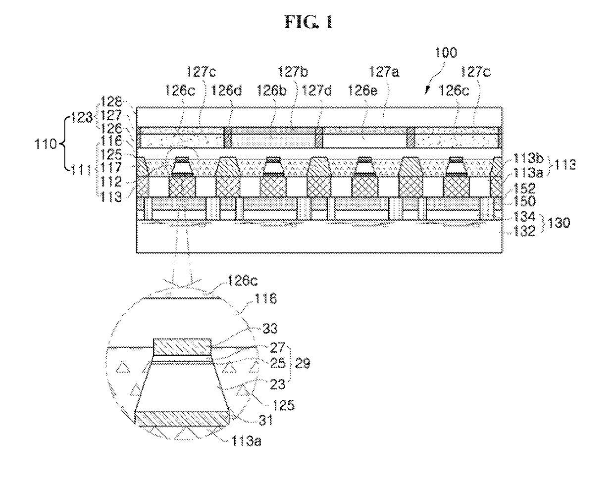
The display apparatus described in this patent uses micro-light emitting diodes made of nitride semiconductors to achieve high resolution, low power consumption, and high efficiency. Additionally, the display apparatus allows for the light emitted from the diodes to be discharged through reflection, reducing the thickness of the light emitting part. When the diodes have a diameter of greater than 10 μm, the display apparatus improves luminous efficacy by allowing light emitted through upper and side surfaces of the diodes to be discharged to the outside. Furthermore, the display apparatus allows multiple light emitting parts to be mounted on a large TFT panel, minimizing failure in manufacture while improving yield.

Problems solved by technology

As a result, the TFT-LCD suffers from constant power consumption regardless of brightness of a displayed screen.
Although power consumption of an OLED display apparatus has been continuously reduced, the OLED still requires a much higher power consumption compared to LEDs formed of inorganic semiconductors.
Thus, OLED based displays generally have power efficiency less than that of LEDs.
Moreover, a passive-matrix (PM) drive type OLED display apparatus can suffer from deterioration in response speed upon pulse amplitude modulation (PAM) of the OLED having large capacitance.
In addition, the PMOLED display apparatus can suffer from deterioration in lifespan upon high current driving through pulse width modulation (PWM) for realizing a low duty ratio.
Thus, the AMOLED display apparatus requires higher manufacturing costs and has non-uniform brightness according to characteristics of TFTs.

Method used


Image

  • Display apparatus
  • Display apparatus
  • Display apparatus

Examples


Embodiment Construction

[0029]In the following description, for the purposes of explanation, numerous specific details are set forth in order to provide a thorough understanding of various exemplary embodiments. It is apparent, however, that various exemplary embodiments may be practiced without these specific details or with one or more equivalent arrangements. In other instances, well-known structures and devices are shown in block diagram form in order to avoid unnecessarily obscuring various exemplary embodiments.

[0030]Unless otherwise specified, the illustrated exemplary embodiments are to be understood as providing exemplary features of varying detail of various exemplary embodiments. Therefore, unless otherwise specified, the features, components, modules, layers, films, panels, regions, and / or aspects of the various illustrations may be otherwise combined, separated, interchanged, and / or rearranged without departing from the disclosed exemplary embodiments. Further, in the accompanying figures, the...


PUM


Abstract

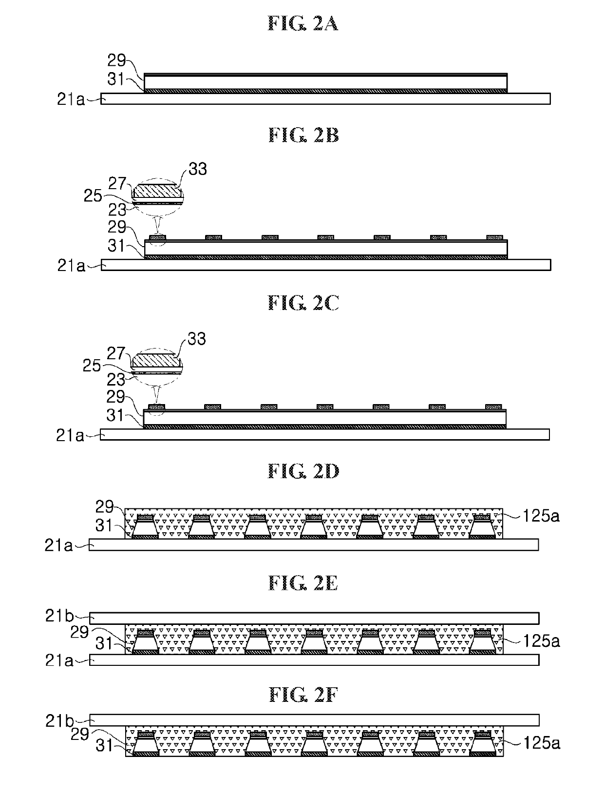
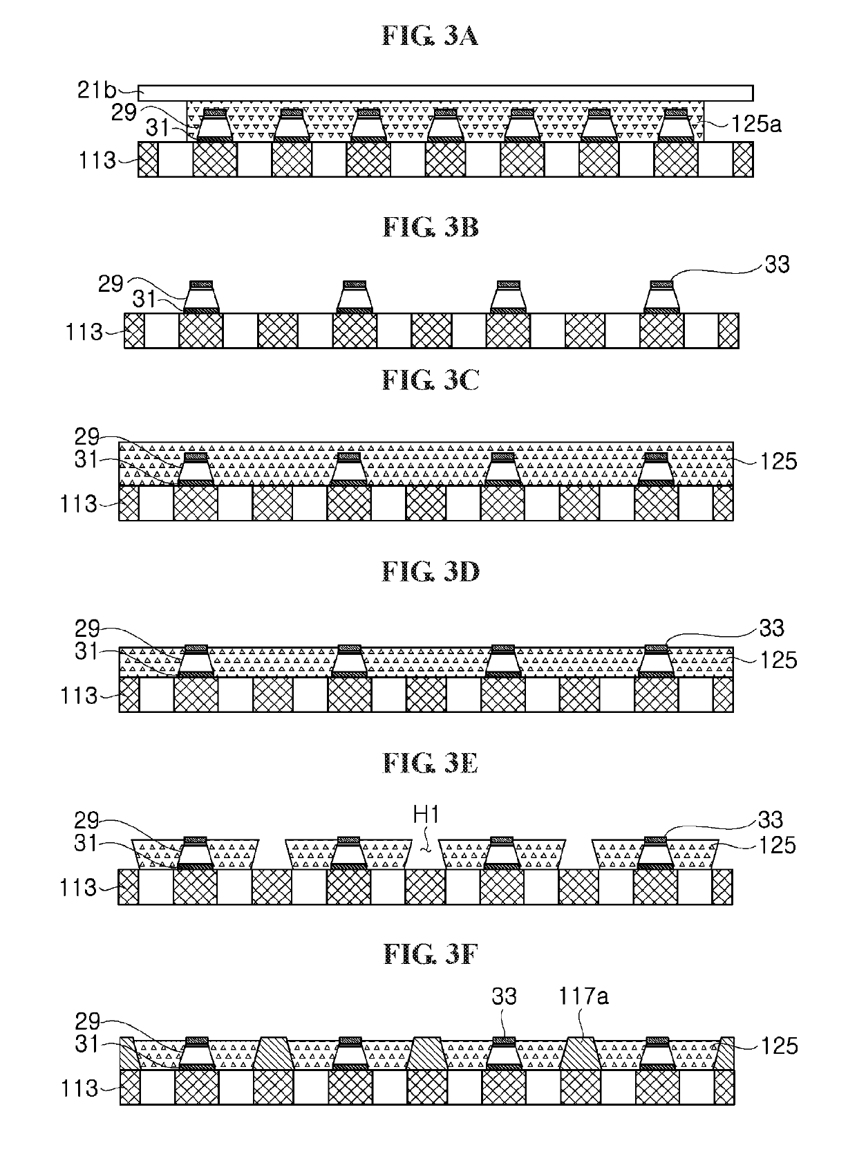
Disclosed are a display apparatus and a method of manufacturing the same. The display apparatus includes a light emitting part including a plurality of light emitting diodes; and a thin film transistor (TFT) panel part configured to drive the plurality of light emitting diodes. A first side of the light emitting part and a first side of the TFT panel part are coupled to each other so as to face each other. The plurality of light emitting diodes are electrically connected to the plurality of TFTs, respectively.

Description

CROSS-REFERENCE TO RELATED APPLICATION[0001]This patent document claims priority to and the benefit of U.S. Patent Provisional Application No. 62 / 358,760, filed on Jul. 6, 2016, which is incorporated by reference for all purposes as if fully set forth herein.BACKGROUNDField[0002]Exemplary embodiments relate to a display apparatus. More particularly, exemplary embodiments relate to a display apparatus using a micro-light emitting diode or a micro-LED.Discussion of the Background[0003]A light emitting diode refers to an inorganic semiconductor device that emits light through recombination of electrons and holes. Due to light emitting diodes having remarkably long lifespans, low power consumption, and rapid response rates, light emitting diodes are also highly versatile. In recent years, light emitting diodes have been used in television displays, monitors, automobile lamps, and general lighting. As a result, a light emitting device has many advantages as a light source.[0004]Recently,...

Claims


Application Information

Patent Timeline
Patent Type & Authority Patents(United States)
IPC IPC(8): H01L25/16H01L51/52H01L27/32
CPCH01L27/3262H01L25/167H01L51/5237H01L51/5203H01L2251/5338H10K59/805H10K59/87H10K59/1213H10K50/84H10K50/805H10K2102/311
Inventor TAKEYA, MOTONOBULEE, JONG IKKIM, YOUNG HYUN
Owner SEOUL SEMICONDUCTOR
Learn More