
Method for producing a conductive multiple substrate stack

a technology of multiple substrates and conductive layers, applied in the direction of photovoltaic energy generation, electrical equipment, semiconductor devices, etc., to achieve the effect of facilitating the connection of two substrates and wide wavelength spectrum

Active Publication Date: 2019-03-26
EV GRP E THALLNER GMBH
View PDF32 Cites 33 Cited by
  • Summary
  • Abstract
  • Description
  • Claims
  • Application Information

AI Technical Summary

Benefits of technology

This method eliminates the need for alignment plants, reduces production costs, and ensures stable and efficient electricity generation by creating a permanent bond with high conductivity and optical transparency, allowing for the connection of substrates with varying wavelength sensitivity.

Problems solved by technology

There are diverse technical problems in the production of conductive multiple-substrate stacks, particularly for generating electricity:generating the greatest amount of electricity possible for the lowest possible area,mass production suitability for the lowest possible costs,long-term stability of the electricity generation,stability with respect to environmental influences, particularly at connection points,reliable electricity generation.

Method used


Image

  • Method for producing a conductive multiple substrate stack
  • Method for producing a conductive multiple substrate stack
  • Method for producing a conductive multiple substrate stack

Examples


Embodiment Construction

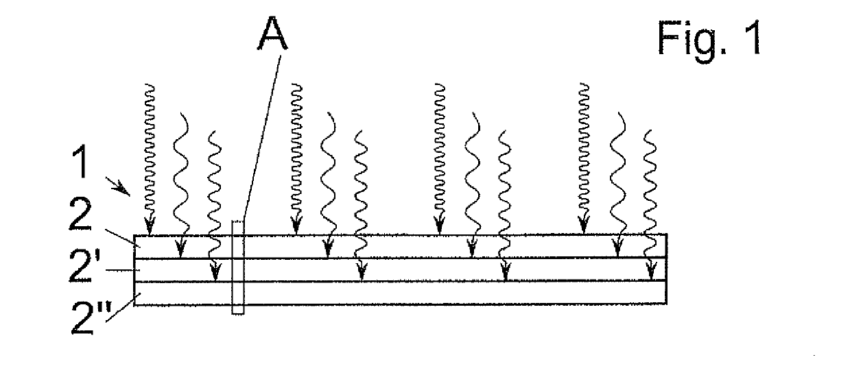
[0097]FIG. 1 shows a schematic cross-sectional view of a substrate stack 1 according to the invention, comprised of three substrates 2, 2′, 2″, The stacking of more or fewer than three substrates 2, 2′, 2″ is also conceivable. The wavelength sensitivity of the substrates is symbolized by wave trains with different wavelength, which represent the electromagnetic waves, in the sense of the partial image, actually the photons. Corresponding contacts for tapping the total voltage generated by the solar cell stack on the outer side are not shown.

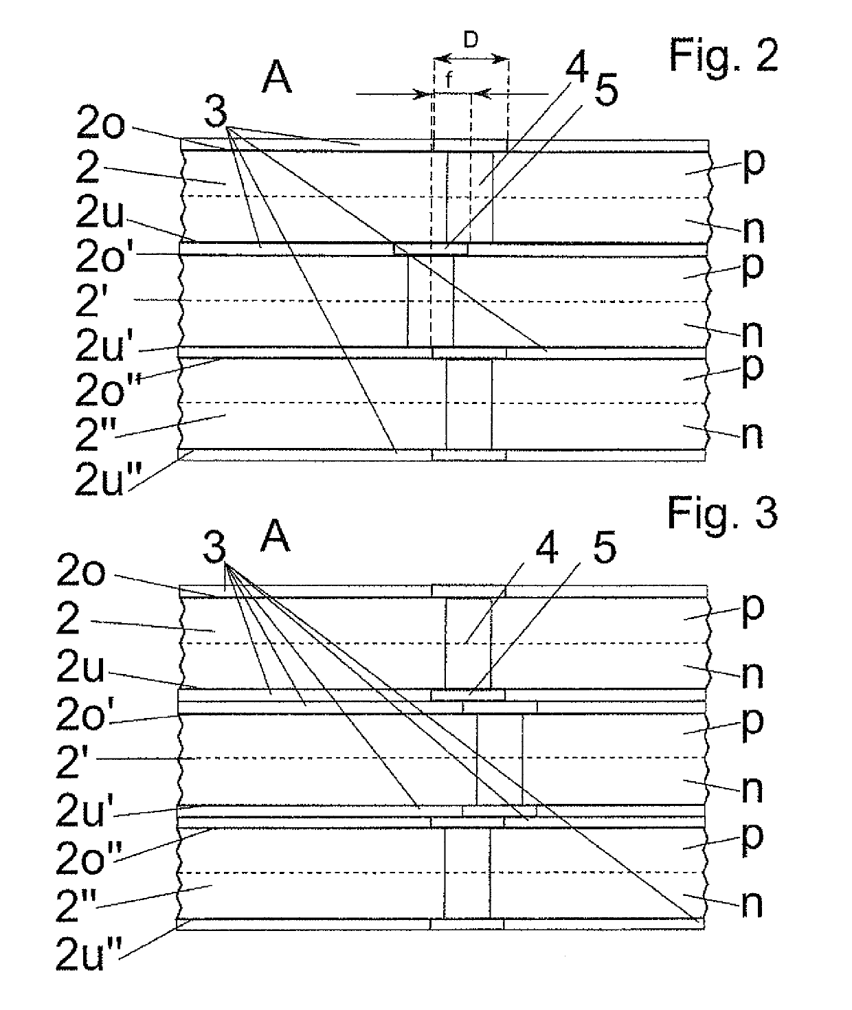
[0098]FIG. 2 shows an enlargement of the section A of the schematic cross-sectional view according to FIG. 1 in a first embodiment according to the invention, in which one can see dielectric layers, particularly oxide layers, 3, by means of which the substrates 2, 2′, 2″ have been connected to one another.

[0099]The dielectric layers 3 alternate in this case between the individual substrates 2, 2′, 2″. This alternation is preferably achieved in su...


PUM


Abstract

A method for producing a multiple-substrate stack from an, in particular wavelength-sensitive, semiconductor substrate and at least one further, in particular wavelength-sensitive, semiconductor substrate with the following steps: applying a dielectric layer, which is electrically conductive at least in certain sections, onto at least one substrate surface of at least one of the semiconductor substrates, and contacting the semiconductor substrate with the further semiconductor substrate and forming an electrically conductive connection between the semiconductor substrates.

Description

FIELD OF THE INVENTION[0001]The invention relates to a method for producing a multiple-substrate stack.BACKGROUND OF THE INVENTION[0002]There are diverse technical problems in the production of conductive multiple-substrate stacks, particularly for generating electricity:[0003]generating the greatest amount of electricity possible for the lowest possible area,[0004]mass production suitability for the lowest possible costs,[0005]long-term stability of the electricity generation,[0006]stability with respect to environmental influences, particularly at connection points,[0007]reliable electricity generation.[0008]The present invention is therefore based on the object of specifying a method, which at least partially, preferably predominantly, solves the aforementioned problems.SUMMARY OF THE INVENTION[0009]The object of the present invention is achieved with the features of the independent claim(s). Advantageous developments of the invention are specified in the dependent claims. All co...

Claims


Application Information

Patent Timeline
Patent Type & Authority Patents(United States)
IPC IPC(8): H01L31/05H01L31/0224H01L21/18H01L25/04H01L31/043
CPCH01L31/0512H01L21/187H01L25/043H01L31/022425H01L31/043Y02E10/50H01L2924/0002H01L2924/00
Inventor MATTHIAS, THORSTEN
Owner EV GRP E THALLNER GMBH
Learn More