
Low noise amplifier circuit

Active Publication Date: 2018-12-04
MELEXIS TECH NV
View PDF3 Cites 5 Cited by
  • Summary
  • Abstract
  • Description
  • Claims
  • Application Information

AI Technical Summary

Benefits of technology

The patent provides an amplifier circuit that can effectively amplify small signals without adding much noise. The circuit was designed to address the problem of reducing noise in analog signals.

Problems solved by technology

Typically several requirements may conflict each other, and thus typically a trade-off needs to be made.

Method used


Image

  • Low noise amplifier circuit
  • Low noise amplifier circuit
  • Low noise amplifier circuit

Examples


first embodiment

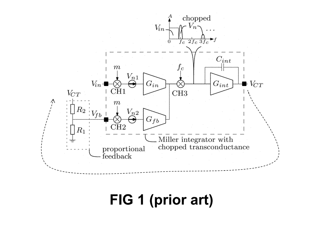
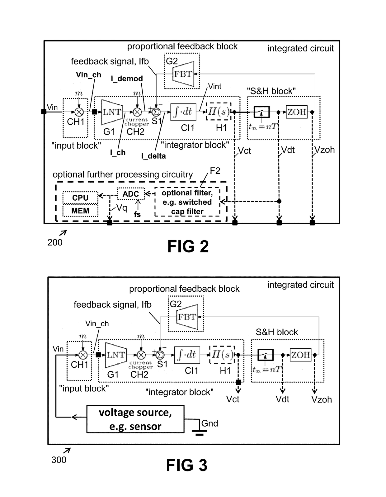
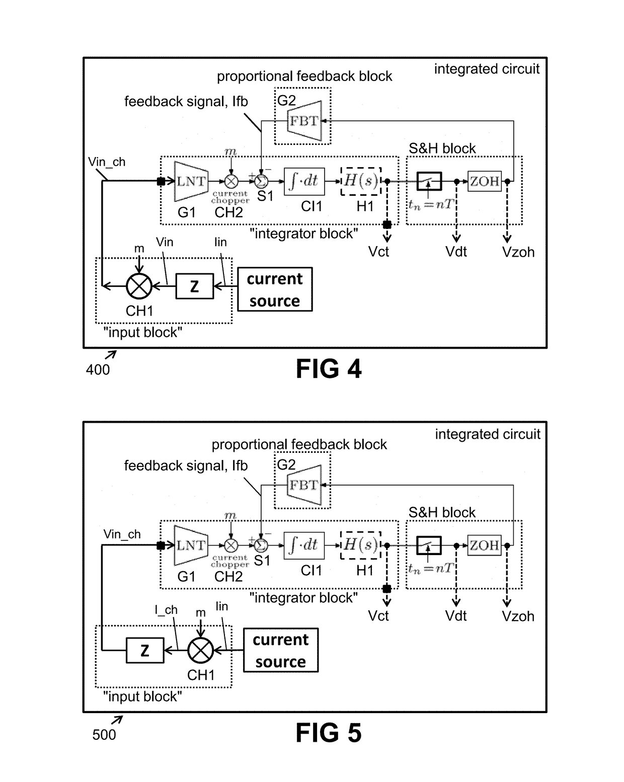
[0121]FIG. 2 shows a high-level block-diagram of a first embodiment of the present invention. FIG. 2 shows a semiconductor circuit comprising an amplifier circuit. The circuit comprises the following blocks:[0122]an input block comprising a first chopper CH1 for providing a chopped input voltage signal Vin_ch indicative of a voltage signal to be amplified;[0123]a first transconductance G1 arranged downstream of the first chopper CH1 and adapted for receiving a chopped voltage signal Vin_ch and adapted for converting said chopped voltage signal into a chopped current signal I_ch;[0124]a second chopper CH2 arranged downstream of the first transconductance G1 adapted for providing a demodulated current signal I_demod;[0125]a current integrator CI1 arranged downstream of the second chopper CH2, the current integrator CI1 comprising an integrating capacitor Cint for storing an integrated signal Vint and being adapted for providing a continuous-time signal Vct;[0126]a first feedback path ...


PUM


Abstract

A semiconductor circuit comprising an input block having a first chopper providing a chopped voltage signal, a first transconductance converting said chopped voltage signal into a chopped current signal, a second chopper providing a demodulated current signal, a current integrator having an integrating capacitor providing a continuous-time signal, a first feedback path comprising: a sample-and-hold block and a first feedback block, the first feedback path providing a proportional feedback signal upstream of the current integrator. The amplification factor is at least 2. Charge stored on the integrating capacitor at the beginning of a sample period is linearly removed during one single sampling period. Each chopper operates at a chopping frequency. The sample-and-hold-block operates at a sampling frequency equal to an integer times the chopping frequency.

Description

FIELD OF THE INVENTION[0001]The present invention relates in general to a low noise amplifier circuit. The present invention is particularly related to a semiconductor circuit comprising such an amplifier circuit, and to a sensor device comprising such an amplifier circuit.BACKGROUND OF THE INVENTION[0002]A large number of amplifier circuits are known in the art. Amplifier circuits are used for many different applications with many different requirements, for example in terms of electrical requirements / constraints: input level, output level, power consumption, heat dissipation, power efficiency, signal bandwidth, signal distortion, noise level, group delay, but also in terms of component cost, PCB size, etc.[0003]Typically several requirements may conflict each other, and thus typically a trade-off needs to be made. There is no single ideal circuit topology which is best for all applications, but each type or class of amplifier has its own advantages and disadvantages.[0004]The pres...

Claims


Application Information

Patent Timeline
Patent Type & Authority Patents(United States)
IPC IPC(8): H03F3/387G01D5/14H03F3/00H03F3/393G01C17/28H03F3/45G01R33/07
CPCH03F3/45475G01D5/142G01R33/07H03F3/005H03F3/387H03F3/393H03F3/45098H03F3/45197G01C17/28H03F2203/45596H03F2200/129H03F2200/135H03F2200/156H03F2200/171H03F2200/261H03F2200/264H03F2200/27H03F2200/271H03F2200/294H03F2200/312H03F2200/321H03F2200/372H03F2200/375H03F2200/81H03F2203/45288H03F2203/45472H03F2203/45496H03F2203/45512H03F2203/45514H03F2203/45528H03F2203/45536H03F2203/45552H03F2203/45564H03F2203/45594H03F1/34
Inventor RAMAN, JOHANROMBOUTS, PIETER
Owner MELEXIS TECH NV
Learn More