Methods of forming semiconductor packages including molding semiconductor chips of the semiconductor packages
a technology of semiconductor chips and semiconductor packages, applied in the field of semiconductor packages, can solve the problems of semiconductor packages becoming more vulnerable under applied forces, semiconductor packages may be damaged or warped under exerted forces, and available semiconductor package structur
- Summary
- Abstract
- Description
- Claims
- Application Information
AI Technical Summary
Benefits of technology
Problems solved by technology
Method used
Image

Examples
Embodiment Construction
[0016]Reference will now be made in detail to the present embodiments of the invention, examples of which are illustrated in the accompanying drawings. Wherever possible, the same reference numbers are used in the drawings and the description to refer to the same or like parts.
[0017]It will be understood that when an element is referred to as being “on” or “over” another element, it can be directly on the other element or intervening elements may be present therebetween. In contrast, when an element is referred to as being “directly on” another element, there are no intervening elements present.
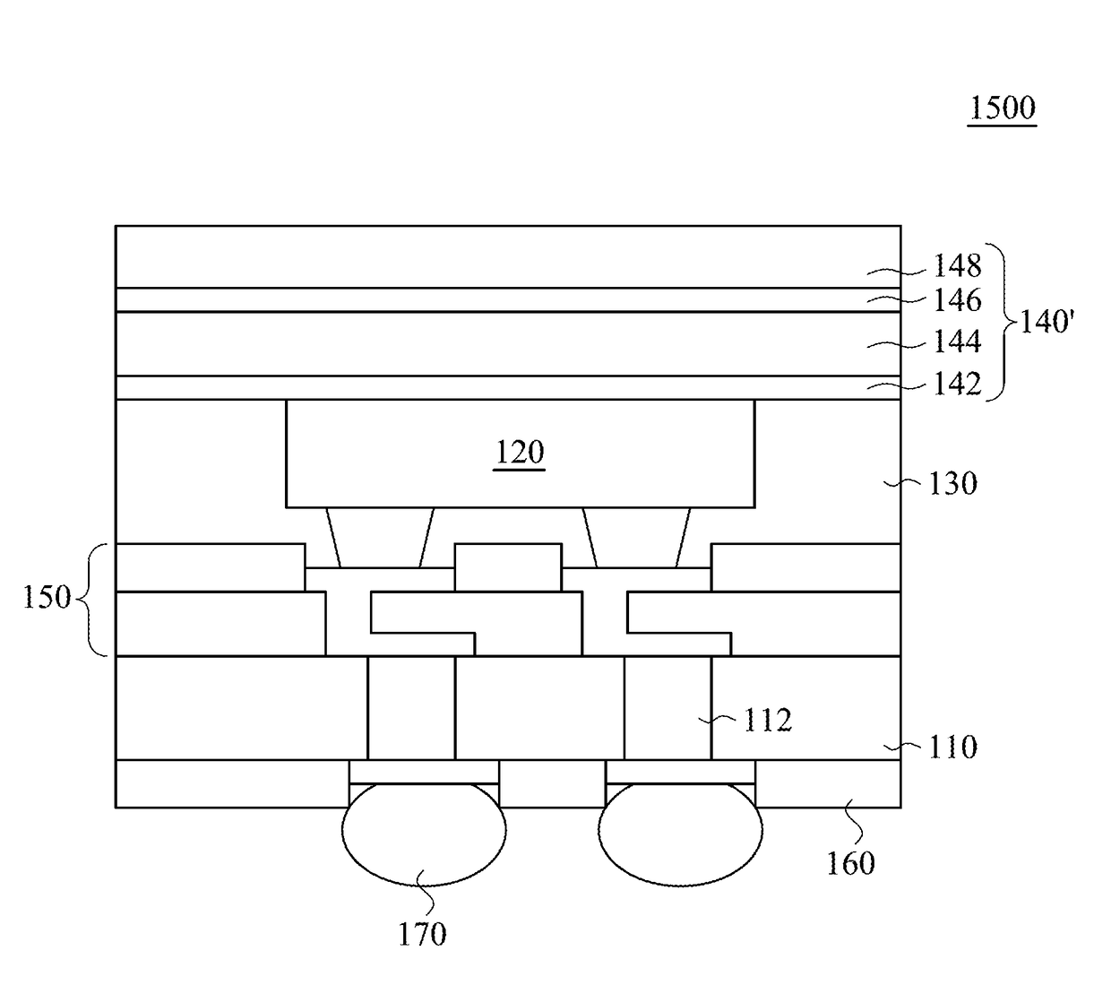
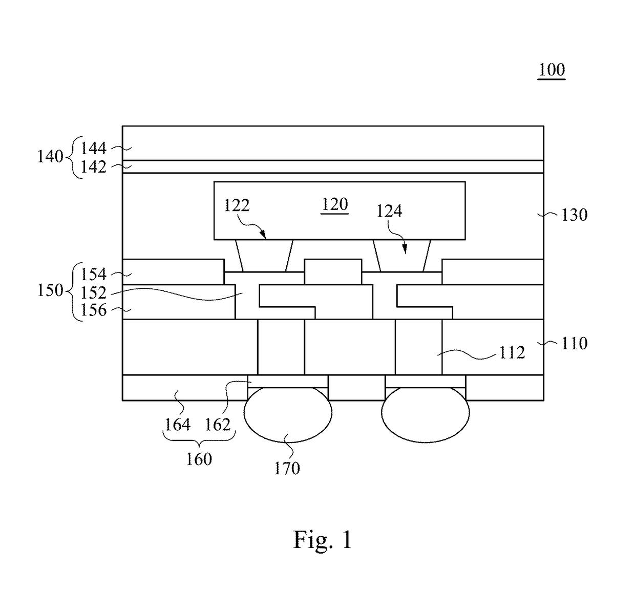
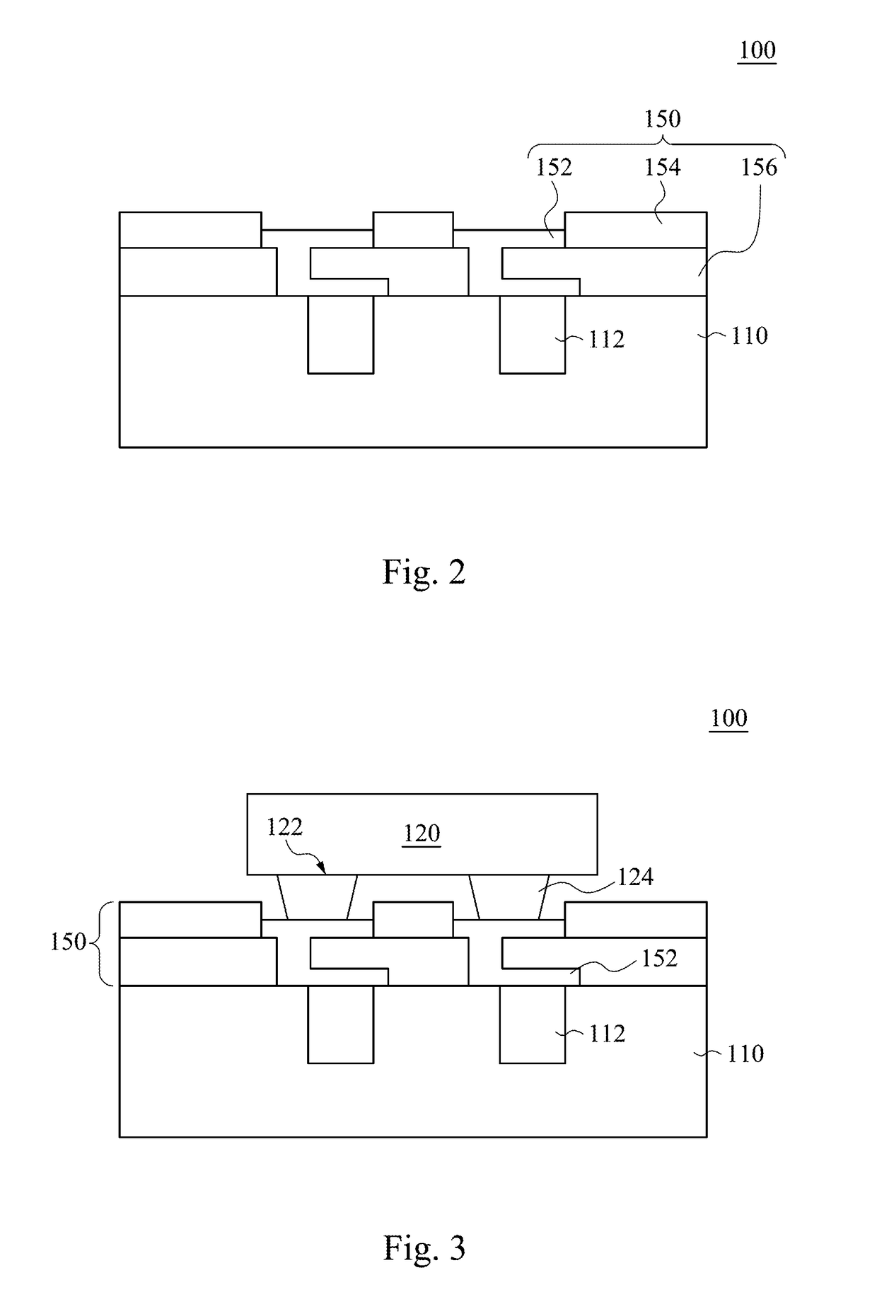
[0018]FIG. 1 illustrates a cross-sectional view of a semiconductor package 100 according to an embodiment of the present disclosure. The semiconductor package 100 includes a wafer 110, a semiconductor chip 120, a first molding material 130, and a composite layer 140. In some embodiments, the wafer 110 of the semiconductor package 100 can also be granted as a substrate. In some embodiments, th...
PUM
 Abstract
Description
Claims
Application Information
 - R&D
- Intellectual Property
- Life Sciences
- Materials
- Tech Scout
- Unparalleled Data Quality
- Higher Quality Content
- 60% Fewer Hallucinations
Browse by: Latest US Patents, China's latest patents, Technical Efficacy Thesaurus, Application Domain, Technology Topic, Popular Technical Reports.
© 2025 PatSnap. All rights reserved.Legal|Privacy policy|Modern Slavery Act Transparency Statement|Sitemap|About US| Contact US: help@patsnap.com