
Touch sensor integrated display device and method for driving the same

a display device and integrated technology, applied in semiconductor devices, instruments, computing, etc., can solve the problems of parasitic capacitance, increase manufacturing cost, and reduce touch sensitivity and touch recognition accuracy, so as to enhance touch sensing capabilities and minimize additional elements

Active Publication Date: 2018-08-21
LG DISPLAY CO LTD
View PDF35 Cites 3 Cited by
  • Summary
  • Abstract
  • Description
  • Claims
  • Application Information

AI Technical Summary

Benefits of technology

This approach minimizes additional elements for touch sensing, improves touch sensitivity and recognition accuracy, and reduces manufacturing costs by integrating touch sensing directly into the display panel without the need for external electrodes or sensor lines.

Problems solved by technology

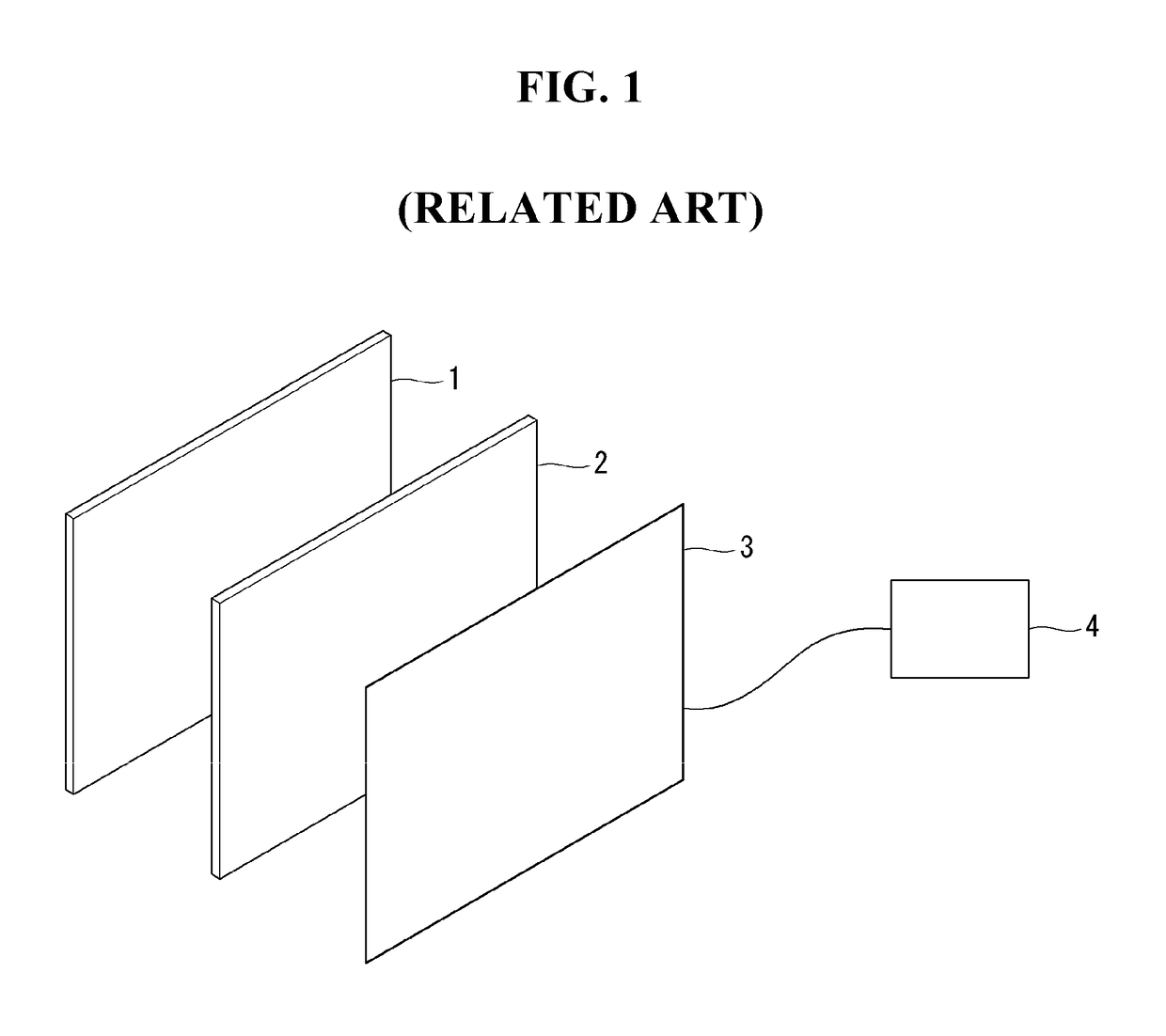
In case of the on-cell type, touch sensors are formed on the upper surface of a display device, with a reduction in thickness compared with the add-on type, but still a driving electrode layer and sensing electrode layer constituting the touch sensors and an insulating film for insulating these layers increase the entire thickness and the number of process steps, leading to an increase in the manufacturing cost.
Moreover, the in-cell type requires an electrode patterning process because an internal electrode used for display is used as an electrode of the touch sensors to achieve a thin profile and has large parasitic capacitance due to the coupling between touch sensors and pixels.
This leads to a reduction in touch sensitivity and touch recognition accuracy.
IR (infrared) sensing does not support multi-touch due to the low response rate and the low touch resolution.
As seen from above, the conventional touch sensor technology requires complicated elements for touch sensing to be added on a display device, which complicates the manufacturing process, increases the manufacturing cost, and lowers touch sensing capabilities.

Method used


Image

  • Touch sensor integrated display device and method for driving the same
  • Touch sensor integrated display device and method for driving the same
  • Touch sensor integrated display device and method for driving the same

Examples


Embodiment Construction

[0092]Hereinafter, various embodiments of a touch sensor integrated display device will be described with reference to FIGS. 3 to 55.

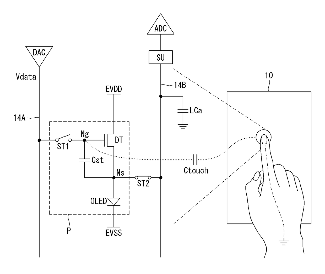
[0093]FIG. 3 is a view showing a touch sensor integrated display device according to one embodiment. FIG. 4 is a view showing a configuration example of a pixel array comprising a plurality of pixels, which can be used as touch sensors, and a source drive IC. FIGS. 5 and 6 are views showing the configuration of a pixel and a configuration example of a sensing unit connected to the pixel according one embodiment.

[0094]The touch sensor integrated display device is implemented as an organic light-emitting display device, especially, one comprising a pixel array for external compensation. The touch sensor integrated display device requires no touch electrodes and sensor lines and can minimize additional elements for touch sensing because it senses touch input using an external compensation-type pixel array.

[0095]External compensation is a technique of sens...


PUM

PropertyMeasurementUnit
threshold voltage Vthaaaaaaaaaa
turn-on voltageaaaaaaaaaa
threshold voltageaaaaaaaaaa

Abstract

A touch sensor integrated display device and a method for driving the same are disclosed. The touch sensor integrated display device includes a display panel, in which a pixel array is divided into a plurality of touch blocks, each touch block includes pixels displaying an input image and a sensing target dummy pixel sensing a touch input, and the sensing target dummy pixel includes a dummy driving TFT configured to control a source-drain current based on a gate-source voltage, and a panel drive circuit, which in a touch sensing period, supplies a scan control signal and a sensing control signal to the sensing target dummy pixel and sets the gate-source voltage to turn on the dummy driving TFT by applying a touch driving data voltage to a gate node of the dummy driving TFT and applying a reference voltage to a source node of the dummy driving TFT.

Description

[0001]This application claims the benefit of Korean Patent Application No. 10-2015-0115033 filed on Aug. 14, 2015, which is incorporated herein by reference for all purposes as if fully set forth herein.BACKGROUND[0002]Related Field[0003]The present disclosure relates to a touch sensor integrated display device and a method for driving the same.[0004]Discussion of the Related Art[0005]Touch sensors are being proposed which enable users to directly touch or get close to the screen and enter data with their finger or a pen while watching displays of a variety of home electronics or data communication devices. The touch sensors are used for various display devices because they are simple to use, have low possibility of malfunction, allow for user input without using an additional input device, and enable the users to operate them quickly and easily through content displayed on the screen.[0006]The touch sensors may be implemented by well-known technologies such as capacitive sensing, i...

Claims


Application Information

Patent Timeline
Patent Type & Authority Patents(United States)
IPC IPC(8): G06F3/041G06F3/044G09G3/3225G09G3/3266H01L27/32G09G3/3233G02F1/1333
CPCG06F3/0418G02F1/13338G06F3/044G06F3/0412H01L27/3223G09G3/3233G09G3/3266H01L27/323G09G3/3225G06F2203/04112G09G2300/0413G09G2300/0426G09G2310/08G09G2320/029G02F1/13624G06F3/0443G02F1/13685H10K59/40H10K59/88
Inventor KIM, TAEGUNGKIM, SEUNGTAEKIM, JUNGHYEON
Owner LG DISPLAY CO LTD
Learn More