Imaging device, module, and electronic device

a technology of imaging device and module, applied in the field of imaging device, can solve the problems of complex process, circuit configuration and operating method of imaging device operating with global shutter method, etc., and achieve the effects of simple circuit configuration, high light sensitivity, and high efficiency of transferring charg

Active Publication Date: 2018-07-03
SEMICON ENERGY LAB CO LTD
View PDF159 Cites 2 Cited by
  • Summary
  • Abstract
  • Description
  • Claims
  • Application Information

AI Technical Summary

Benefits of technology

[0010]When the data retention portion is provided, a transfer gate needs to be provided in the data retention portion for accurate readout of imaging data. To increase the efficiency of transferring charge corresponding to imaging data, the transfer gate preferably overlaps a gate electrode of a transfer transistor or the like; however, this structure makes the process complicated, compared to a structure where the transfer gate does not overlap such a gate electrode.
[0011]In view of the above, an object of one embodiment of the present invention is to provide an imaging device with high efficiency of transferring charge corresponding to imaging data. Another object is to provide an imaging device with high light sensitivity. Another object is to provide an imaging device with a simple circuit configuration. Another object is to provide an imaging device that operates through a simple procedure. Another object is to provide an imaging device capable of being manufactured in a simple process. Another object is to provide an imaging device capable of capturing an image of a moving object without distortion. Another object is to provide an imaging device capable of retaining data for a long time. Another object is to provide an imaging device with high resolution. Another object is to provide a small-sized imaging device. Another object is to provide an imaging device suitable for high-speed operation. Another object is to provide an imaging device with high reliability. Another object is to provide an imaging device capable of being manufactured at low cost. Another object is to provide a novel imaging device or the like.
[0021]One embodiment of the present invention can provide an imaging device with high efficiency of transferring charge corresponding to imaging data, an imaging device with high light sensitivity, an imaging device with a simple circuit configuration, an imaging device that operates through a simple procedure, an imaging device capable of being manufactured in a simple process, an imaging device capable of capturing an image of a moving object without distortion, an imaging device capable of retaining data for a long time, an imaging device with high resolution, a small-sized imaging device, an imaging device suitable for high-speed operation, an imaging device with high reliability, an imaging device capable of being manufactured at low cost, a novel imaging device, or the like.

Problems solved by technology

Accordingly, a circuit configuration and an operating method of an imaging device operating with the global shutter method are more complicated than those of an imaging device operating with a rolling shutter method.
To increase the efficiency of transferring charge corresponding to imaging data, the transfer gate preferably overlaps a gate electrode of a transfer transistor or the like; however, this structure makes the process complicated, compared to a structure where the transfer gate does not overlap such a gate electrode.

Method used


Image

  • Imaging device, module, and electronic device
  • Imaging device, module, and electronic device
  • Imaging device, module, and electronic device

Examples


embodiment 1

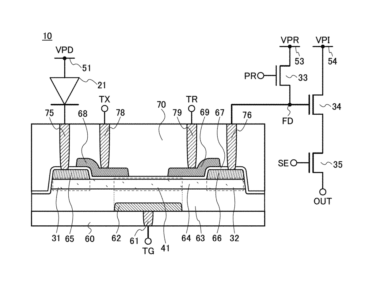
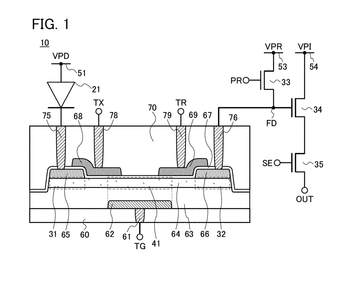
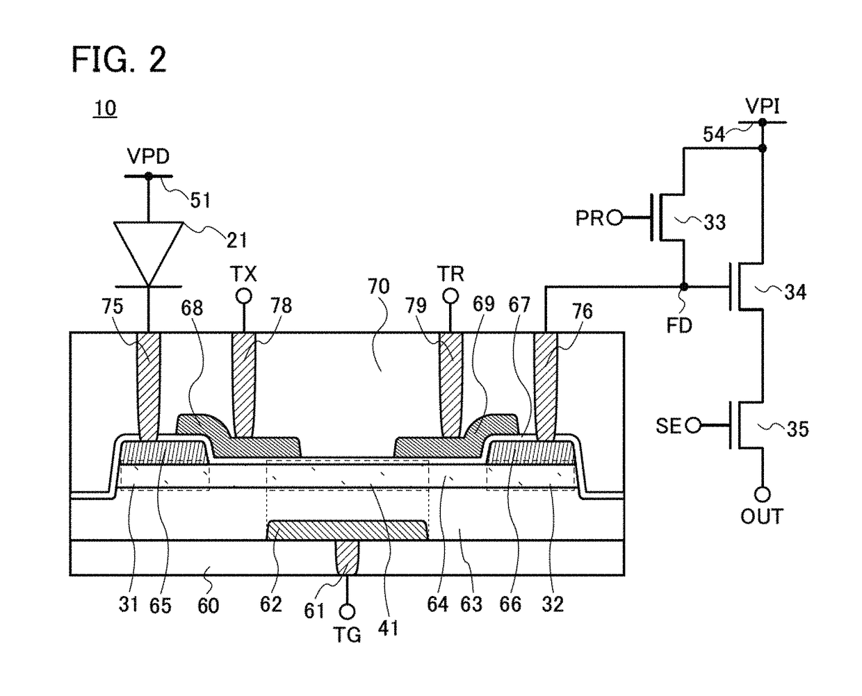
[0080]In this embodiment, an imaging device that is one embodiment of the present invention will be described with reference to drawings.

[0081]FIG. 1 illustrates a cross-sectional view and a circuit diagram that show a structure example of a pixel 10 included in an imaging device of one embodiment of the present invention. Although FIG. 1 and the like show an example using n-channel transistors, one embodiment of the present invention is not limited to this, and some transistors may be replaced with p-channel transistors.

[0082]The pixel 10 includes a conductor 62 in contact with an insulator 60; an insulator 63 in contact with the conductor 62; a semiconductor 64 in contact with the insulator 63; a conductor 65 and a conductor 66 in contact with the semiconductor 64; an insulator 67 in contact with the insulator 63, the semiconductor 64, and the conductors 65 and 66; a conductor 68 and a conductor 69 in contact with the insulator 67; and an insulator 70 in contact with the insulator...

embodiment 2

[0227]In this embodiment, an OS transistor that can be used in one embodiment of the present invention will be described with reference to drawings. In the drawings in this embodiment, some components are enlarged, reduced in size, or omitted for easy understanding.

[0228]FIGS. 22A to 22C are a top view and cross-sectional views of a transistor 301 of one embodiment of the present invention. FIG. 22A is the top view. FIG. 22B shows a cross section along the dashed-dotted line X1-X2 in FIG. 22A. FIG. 22C shows a cross section along the dashed-dotted line Y1-Y2 in FIG. 22A.

[0229]In the drawings explained in this embodiment, the direction of the dashed-dotted line X1-X2 is referred to as channel length direction, and the direction of the dashed-dotted line Y1-Y2 is referred to as channel width direction.

[0230]The transistor 301 includes a conductor 320 in contact with the substrate 310, an insulator 330 in contact with the substrate 310 and the conductor 320, an oxide semiconductor 340 ...

embodiment 3

[0274]In this embodiment, components of the transistors shown in Embodiment 2 will be described in detail.

[0275]As the substrate 310, a glass substrate, a quartz substrate, a semiconductor substrate, a ceramic substrate, a metal substrate with an insulated surface, or the like can be used. Other examples are a silicon substrate provided with a transistor and / or a photodiode; and a silicon substrate over which an insulator, a wiring, a conductor functioning as a contact plug, and the like are provided together with a transistor and / or a photodiode. When a p-channel transistor is formed on a silicon substrate, a silicon substrate with n−-type conductivity is preferably used. Alternatively, an SOI substrate including an n−-type or i-type silicon layer may be used. Moreover, when a p-channel transistor is formed on a silicon substrate, a surface of the silicon substrate where the transistor is formed preferably has a (110) plane orientation, in which case the mobility can be increased.

[...


PUM


Abstract

An object is to provide an imaging device with high efficiency of transferring charge corresponding to imaging data. The imaging device includes first to fifth conductors, first and second insulators, an oxide semiconductor, a photoelectric conversion element, and a transistor. The first conductor is in contact with a bottom surface and a side surface of the first insulator. The first insulator is in contact with a bottom surface of the oxide semiconductor. The oxide semiconductor is in contact with bottom surfaces of the second and third conductors and the second insulator. Each of the second and third conductors is in contact with the bottom surface and a side surface of the second insulator. The second insulator is in contact with bottom surfaces of the fourth and fifth conductors. The first conductor has regions overlapped by the fourth and fifth conductors. The second conductor has a region overlapped by the fourth conductor. The third conductor has a region overlapped by the fifth conductor. The second conductor is electrically connected to one electrode of the photoelectric conversion element. The third conductor is electrically connected to a gate of the transistor.

Description

BACKGROUND OF THE INVENTION[0001]1. Field of the Invention[0002]One embodiment of the present invention relates to an imaging device.[0003]Note that one embodiment of the present invention is not limited to the above technical field. The technical field of one embodiment of the invention disclosed in this specification and the like relates to an object, a method, or a manufacturing method. Furthermore, one embodiment of the present invention relates to a process, a machine, manufacture, or a composition of matter. Specific examples of the technical field of one embodiment of the present invention disclosed in this specification include a semiconductor device, a display device, a liquid crystal display device, a light-emitting device, a lighting device, a power storage device, a memory device, an imaging device, a method for operating any of them, and a method for manufacturing any of them.[0004]In this specification and the like, a semiconductor device generally means a device that ...

Claims


Application Information

Patent Timeline
Patent Type & Authority Patents(United States)
IPC IPC(8): H01L27/00H01L27/146H01L29/786H04N5/353H04N5/235H04N5/378
CPCH01L27/14616H01L27/14609H01L27/14612H01L27/14614H01L27/14627H01L27/14636H01L27/14643H01L29/7869H01L27/14634H04N5/378H04N5/2353H04N5/353H01L27/14638H01L2224/48091H01L27/146H01L27/1463H04N25/53H01L2924/00014H01L27/1214H04N23/73H04N25/75H10K39/32
Inventor IKEDA, TAKAYUKI
Owner SEMICON ENERGY LAB CO LTD
Why Eureka
Try Eureka