Functional molecular element, method for producing functional molecular element, and functional molecular device
A technology of molecular components and molecular devices, applied in semiconductor/solid-state device manufacturing, electrical components, electric solid-state devices, etc., can solve problems such as the inability to improve the specific properties of molecular devices, large resistance, etc.
- Summary
- Abstract
- Description
- Claims
- Application Information
AI Technical Summary
Problems solved by technology
Method used
Image

Examples
no. 1 approach
[0088] The first embodiment mainly concerns functional molecular elements corresponding to claims 1-3.
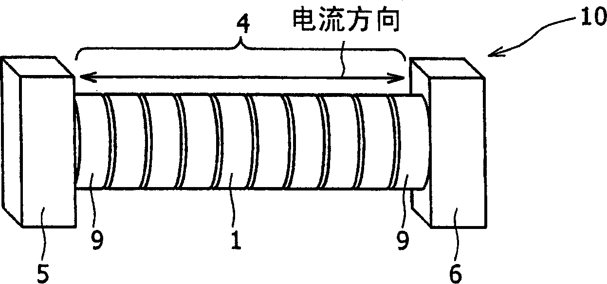
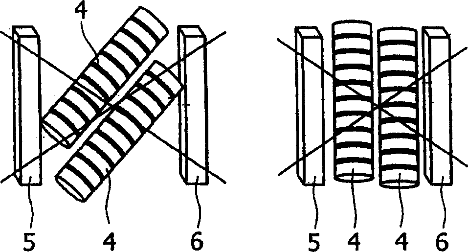
[0089] Figure 1A is a schematic diagram of the functional molecular element 10 according to the first embodiment. Figure 1B is a schematic diagram of a comparative example. Figure 1C It is a schematic diagram illustrating the orientation of π-electron conjugated molecules 1 (or adsorbed molecules 9 on electrodes) in the first molecular layer constituting the array structure 4 of the functional molecular element 10 . figure 2 is the structural formula of the π-electron conjugated molecule 1 constituting the array structure 4 .
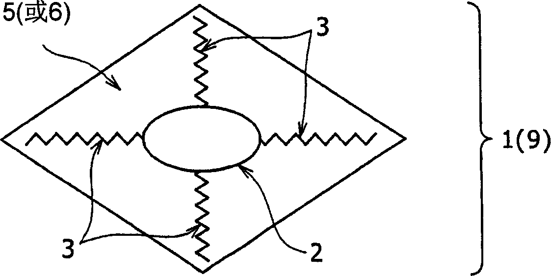
[0090] Such as figure 2 Said, the skeleton 2 of the π-electron conjugated molecule 1 is based on dimethylbilinone (or 4,9-dimethylbilin-1-one). Dimethicone is a linear tetrapyrrole whose structure corresponds to an open porphyrin ring. The π-electron conjugated molecule 1 consists of a backbone 2 and a side chain 3 (p-alkylphenyl) attached t...
no. 2 approach
[0103] The second embodiment is mainly concerned with a functional molecular device corresponding to claims 1-3 and 17-20, which device is an insulated gate field effect transistor, wherein the functional molecular element 10 (the element described in the first embodiment) is held between opposing electrodes. image 3 It is a cross-sectional view explaining the structure of the insulated gate field effect transistor 20 of this embodiment.
[0104] image 3 The shown insulated gate field effect transistor 20 is formed on a doped silicon substrate 11 which also serves as a gate 13 for controlling current flow. A gate insulating film 12 (or a silicon oxide film) is formed on the surface of the silicon substrate 11 . There are opposing gold electrodes (or source electrode 14 and drain electrode 15 ) on gate insulating film 12 . Between these electrodes is the array structure 4 described in the first embodiment.
[0105] Of the π-electron conjugated molecules 1 constituting the...
no. 3 approach
[0112] The third embodiment mainly relates to functional molecular elements corresponding to claims 1, 4 and 5, and functional molecular devices corresponding to claims 17-20, which are insulated gate field effect transistors.
[0113] Figure 4A and 4B are schematic structures showing π-electron conjugated molecules 1 and 31 constituting the functional molecular elements of Embodiments 1 and 3, respectively.
[0114] Figure 4A The part on the left is a schematic diagram showing the three-dimensional structure of the approximately flat circular skeleton 2 of the π-electron conjugated molecule 1 . In this figure, the carbon atoms, nitrogen atoms, oxygen atoms and metal ions M constituting the skeleton 2 are represented by spheres, the hydrogen atoms are omitted in the figure, and the side chain 3 is simplified. The π-electron conjugated molecule 1 has two opposing carbonyl groups (C=O) at the cleavage of the open porphyrin ring. Therefore, the skeleton 2 has an approximate...
PUM
 Abstract
Description
Claims
Application Information
 - R&D
- Intellectual Property
- Life Sciences
- Materials
- Tech Scout
- Unparalleled Data Quality
- Higher Quality Content
- 60% Fewer Hallucinations
Browse by: Latest US Patents, China's latest patents, Technical Efficacy Thesaurus, Application Domain, Technology Topic, Popular Technical Reports.
© 2025 PatSnap. All rights reserved.Legal|Privacy policy|Modern Slavery Act Transparency Statement|Sitemap|About US| Contact US: help@patsnap.com