
Semiconductor integrated circuit device and its power supply wiring method

A technology for power supply wiring and integrated circuits, applied in semiconductor devices, semiconductor/solid-state device manufacturing, circuits, etc., can solve problems such as high power consumption, reduced LSI reliability, and inability to fully alleviate them

Inactive Publication Date: 2006-03-29
SANYO ELECTRIC CO LTD
View PDF1 Cites 3 Cited by
  • Summary
  • Abstract
  • Description
  • Claims
  • Application Information

AI Technical Summary

Problems solved by technology

[0005] However, due to the rapid increase in scale and high integration of LSIs in recent years, the miniaturization of wiring and the extension of wiring length have made it difficult for the above-mentioned conventional power supply wiring to sufficiently alleviate the IR drop.
[0006] In addition, the current density of the power supply wiring may exceed the local allowable current density in the part that consumes a large amount of power in the logic circuit section.
Excessive current density is the cause of electromigration, therefore, violation of the current density limit will cause a decrease in the reliability of LSI

Method used


Image

  • Semiconductor integrated circuit device and its power supply wiring method
  • Semiconductor integrated circuit device and its power supply wiring method
  • Semiconductor integrated circuit device and its power supply wiring method

Examples


Embodiment Construction

[0085] Hereinafter, a related semiconductor integrated circuit device (LSI) and its power supply wiring method according to the first embodiment of the present invention will be described with reference to the drawings.

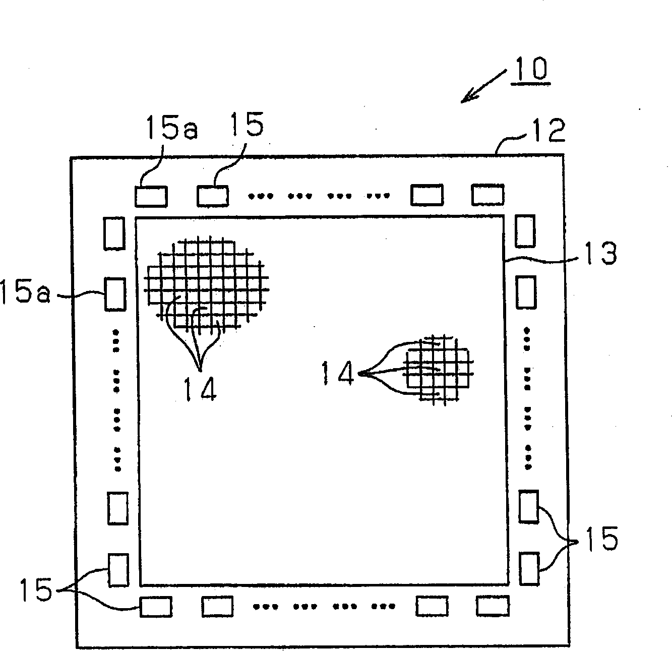
[0086] As shown in FIG. 2( a ), the LSI 10 has a square logic circuit unit 13 provided on a substrate 12 . The logic circuit unit 13 is composed of a plurality of cells 14 . A plurality of pads 15 are provided on the substrate 12 along the outer periphery of the logic circuit portion 13 . Some pads 15 function as power supply pads (power supply section, power supply origin) 15 a for supplying power to the logic circuit section 13 . The power supply unit may be provided above or below the logic circuit unit 13 .

[0087] As shown in FIG. 2( b ), a ring-shaped power supply wiring surrounding the logic circuit unit 13 , that is, a power supply loop 16 is wired. The power supply loop 16 is electrically connected to the power supply pad 15 a through the lead wi...


PUM


Abstract

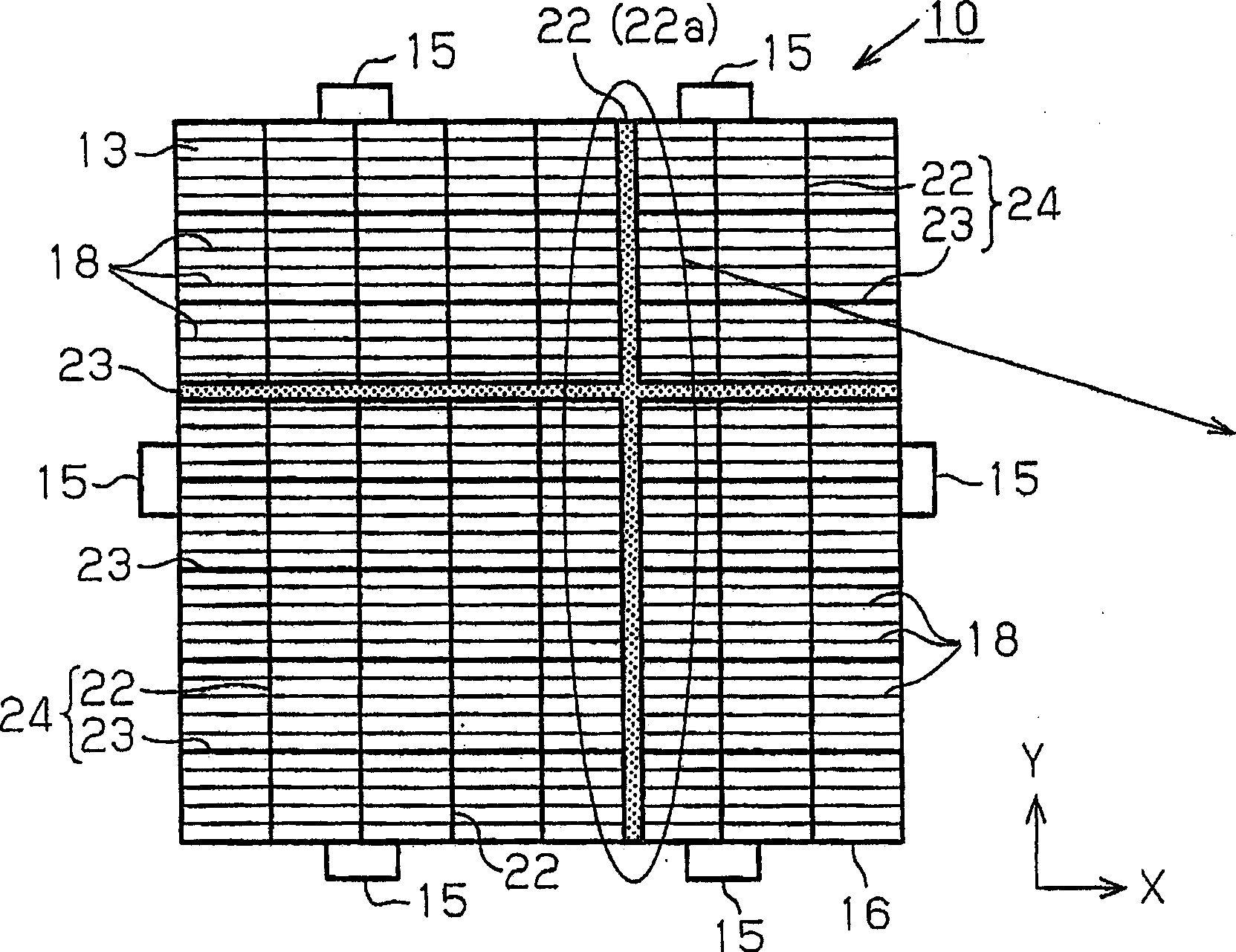
A wiring method of power supply for a semiconductor integrated circuit device operating stably. A power supply mesh (24) provided in a layer overlying a basic power supply wiring (18) for supplying power to a logic circuit section (13) includes a longitudinal reinforcing power supply wiring (22) and a lateral reinforcing power supply wiring (23). Widths of the longitudinal reinforcing power supply wiring (22) and the lateral reinforcing power supply wiring (23) are optimized to relax an IR drop or an excessive current density for each division unit u0.

Description

technical field [0001] The invention relates to a semiconductor integrated circuit device and a power wiring method thereof. Background technique [0002] With the increase in scale and high integration of semiconductor integrated circuits (LSI), the voltage drop inside the logic circuit (for example, near the center) due to the increase in impedance of the power supply wiring that supplies the operating current to the logic circuit ( IR drop) becomes quite significant. The voltage drop of the power supply wiring is a problem that cannot be ignored, causing the response speed of the logic gate circuit to decrease and malfunction. Therefore, in the conventional LSI, in addition to the basic power supply wiring for supplying direct power to the logic circuit part, there is also a reinforced power supply wiring to increase the total wiring width, thereby alleviating the IR drop (see JP-A-2002-261245 ) [0003] Figure 91 It is a plan view illustrating power supply wiring of ...

Claims


Application Information

Patent Timeline
Patent Type & Authority Applications(China)
IPC IPC(8): H01L21/82H01L27/04G06F17/50
Inventor 斋田敦向野守
Owner SANYO ELECTRIC CO LTD
Learn More