Thin film transistor array for a liquid crystal display

A liquid crystal display, pixel column technology, applied in instruments, identification devices, nonlinear optics, etc., can solve the problems of uneven pixel polarity, flicker and pixel column brightness differences, and reduce the image quality of display devices.

Inactive Publication Date: 2005-05-04
SAMSUNG DISPLAY CO LTD
View PDF0 Cites 11 Cited by
  • Summary
  • Abstract
  • Description
  • Claims
  • Application Information

AI Technical Summary

Problems solved by technology

But in this case, the pixel polarity becomes non-uniform with respect to red, green and blue pixels and simultaneously produces flickering and brightness differences between pixel columns
This degrades the image quality of the resulting display device

Method used


Image

  • Thin film transistor array for a liquid crystal display
  • Thin film transistor array for a liquid crystal display
  • Thin film transistor array for a liquid crystal display

Examples


Embodiment Construction

[0038] Preferred embodiments of the present invention will be described in detail below with reference to the accompanying drawings.

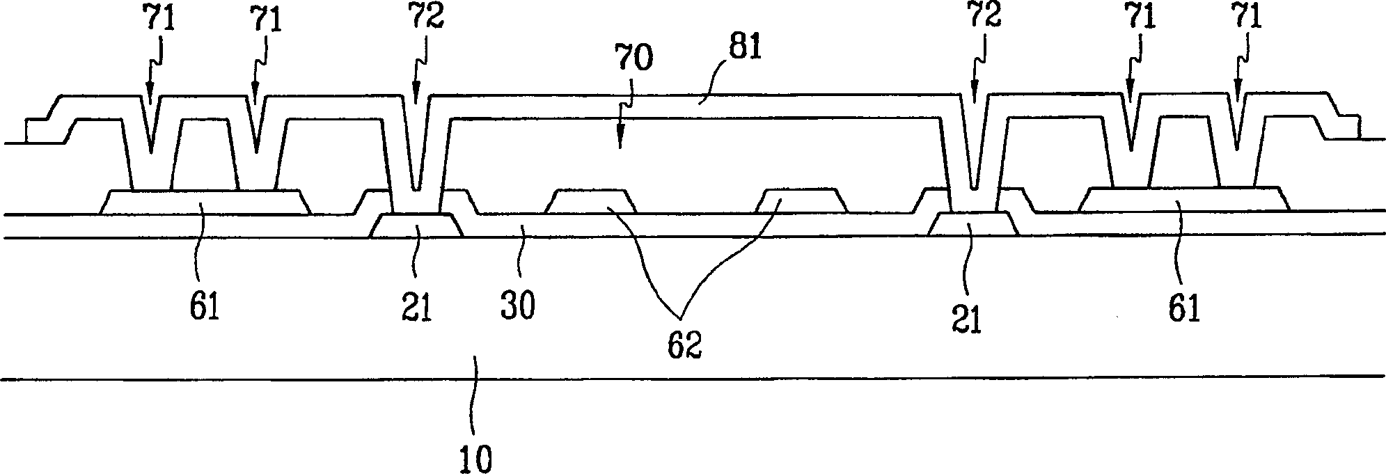
[0039] figure 1 is a plan view of a thin film transistor array panel for a liquid crystal display according to a first preferred embodiment of the present invention, figure 2 and 3 is the thin film transistor array edge figure 1 Cross-sectional views of lines II-II' and III-III'. figure 2 Specifically, a pixel region and a pad region are shown. image 3 Represents a connection unit C for interconnecting a data line for transmitting a data signal to adjacent blue pixels B1 and B2 through a pad.

[0040] Such as figure 1 As shown, the red, blue and green pixels R, B1, G, R, B2 and G are distributed in a matrix form on the thin film transistor array board for liquid crystal display. The red, blue and green pixels R, B1, G, R, B2 and G are sequentially distributed in the row direction, and the pixels of the same color are adjacent in the co...


PUM


Abstract

Pixels of red, blue and green are sequentially arranged in the row direction. The red and green pixels are alternately arranged in the column while the blue pixels being arranged between the neighboring red and each blue pixel is surrounded by the four red and green pixels. Gate lines are arranged at respective pixel rows. Data lines cross over the gate lines in an insulating manner and are arranged at the respective pixel columns. Pixel electrodes and thin film transistor are arranged at the respective pixels. At a predetermined pixel unit, the data lines to the two blue pixel are connected to each other. The pixel electrodes are overlapped with the gate lines or data lines via a passivation layer of low dielectric organic material or insulating material such as SiOC, SiOF.

Description

technical field [0001] The invention relates to a liquid crystal display. Background technique [0002] Generally, a liquid crystal display has two substrates with electrodes and a liquid crystal layer sandwiched between the two substrates. Applying a voltage to the electrodes causes the liquid crystal molecules in the liquid crystal layer to reorientate, thereby controlling the transmission of light. [0003] Liquid crystal displays have multiple pixels with pixel electrodes and red, green and blue color filters. The pixels are driven by signals applied via wiring. The wiring includes scan signal lines or gate lines for carrying scan signals, and image signal lines or data lines for carrying image signals. Thin film transistors are formed at each pixel and are connected to one gate line and one data line. Image signals applied to the pixel electrodes are controlled by thin film transistors. [0004] There are several types of color filter layouts for red, green, and bl...

Claims


Application Information

Patent Timeline
Patent Type & Authority Applications(China)
IPC IPC(8): G02F1/1335G02F1/1343G02F1/1368G09F9/30G09F9/35
CPCG02F1/133514G02F2201/52
Inventor 洪雯勺洪完植卢南锡丁奎夏蔡钟哲
Owner SAMSUNG DISPLAY CO LTD
Why Eureka
Try Eureka