Carbon nano tube NOR logic device

A logic device and carbon nanotube technology, applied in the field of logic devices, can solve the problems of complex device structure and difficult fabrication, and achieve the effects of simple device structure, easy fabrication materials, and easy fabrication and integration.

Inactive Publication Date: 2006-01-11
INST OF PHYSICS - CHINESE ACAD OF SCI
View PDF0 Cites 0 Cited by
  • Summary
  • Abstract
  • Description
  • Claims
  • Application Information

AI Technical Summary

Problems solved by technology

[0006] The purpose of the present invention is to overcome the defect that the existing logic device uses two carbon nanotubes, and each carbon nanotube has an independent gate, which causes the device structure to be complex and difficult to manufacture; in order to solve the difficulty of device manufacture, Reducing the structural complexity of carbon nanotube "or-no" logic devices, thereby providing a carbon nanotube "or-no" logic device

Method used


Image

  • Carbon nano tube NOR logic device
  • Carbon nano tube NOR logic device
  • Carbon nano tube NOR logic device

Examples


Embodiment 1

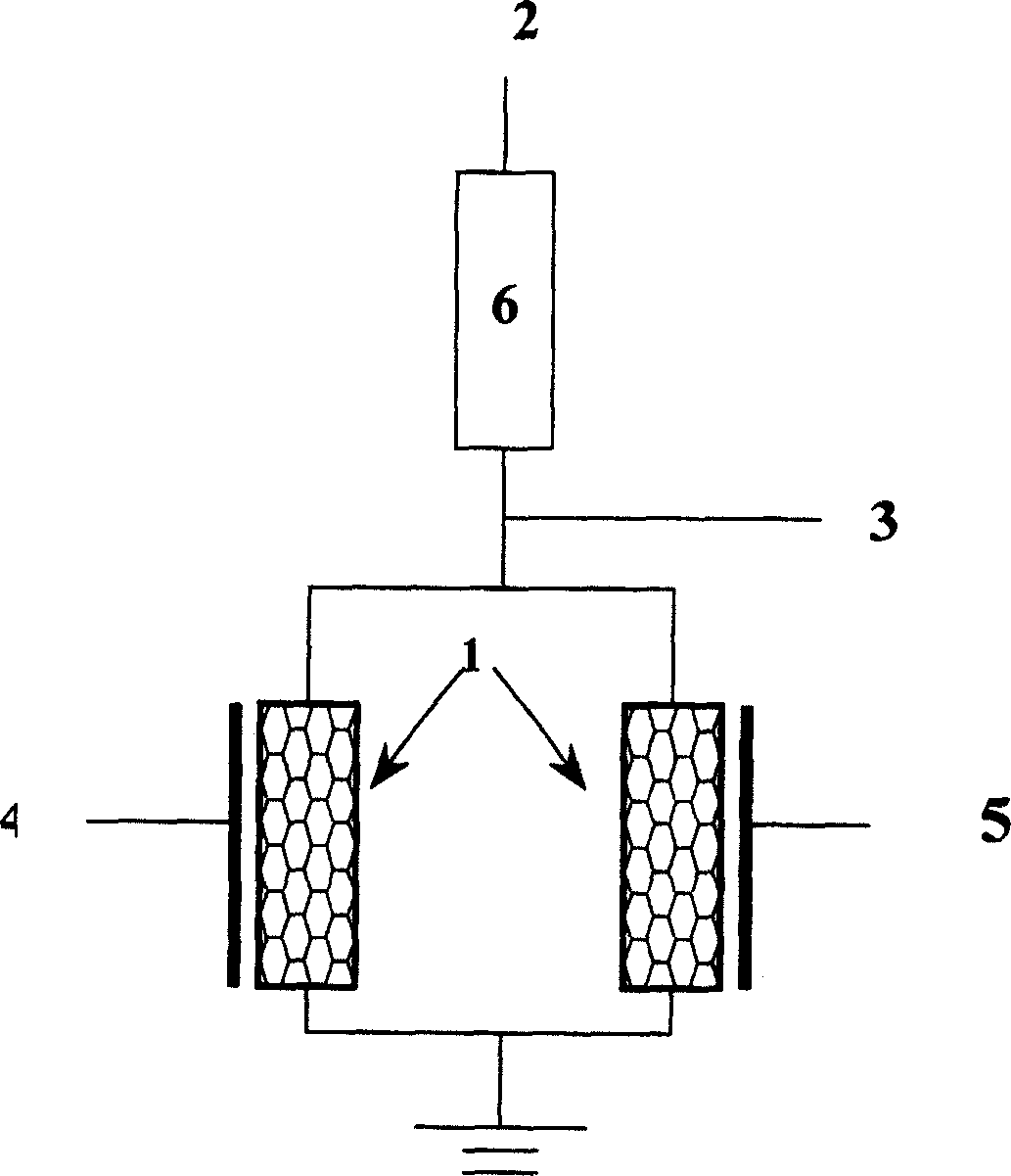
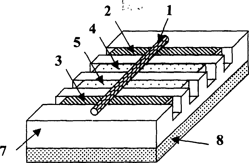
[0027] refer to figure 2 , 3 and 4, the structure of the carbon nanotube "or-no" logic device of the present invention is described in detail in combination with the manufacturing method and the embodiment:

[0028] Silicon with (001) orientation is selected as the substrate 8 . Form 300nm thick SiO by using organic vapor phase deposition method (PECVD) 2 insulating layer7. In SiO 2 Electron photoresist (PMMA) with a thickness of 80 nm is evenly covered on the insulating layer 7 . After the photoresist is exposed, two trenches with a width of 30 nm and a distance of 50 nm are formed on the photoresist. Applying dry etching, the SiO exposed in the photoresist 2 Grooves with a width of 30 nm and a depth of 30 nm are etched on the insulating layer 7 for making gates 4 and 5 . A layer of Al with a thickness of 30nm is deposited on the surface by electron beam evaporation method. After stripping and cleaning, the intrinsic oxidation method is used to form 2-3nm thick Al on...

Embodiment 2

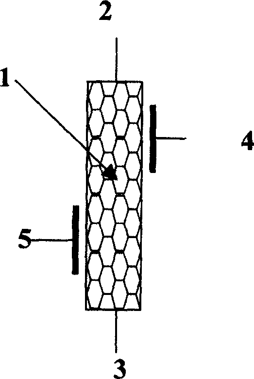
[0049] refer to image 3 , 4 and Figure 5 , the structure of this embodiment is described in detail in conjunction with the manufacturing method:

[0050] Silicon with (001) orientation is selected as the substrate 8 . Form 300nm thick SiO by using organic vapor deposition method (PECVD) 2 insulating layer7. In SiO 2 Electron photoresist (PMMA) with a thickness of 80nm is evenly covered on the insulating layer 7; after the photoresist is exposed, two grooves with a width of 30nm and a distance of 50nm are formed on the photoresist. Using dry etching, the photoresist exposed SiO 2 A groove with a width of 30 nm and a depth of 30 nm is etched on the insulating layer 7 . A layer of Al with a thickness of 30nm is deposited on the surface by electron beam evaporation method. After stripping and cleaning, the intrinsic oxidation method is used to form 2-3nm thick Al on the Al surface. 2 o 3 Insulation. In this way, the preparation of the first grid 4 and the second grid ...


PUM

PropertyMeasurementUnit
thicknessaaaaaaaaaa
thicknessaaaaaaaaaa
thicknessaaaaaaaaaa

Abstract

This invention relates to a carbon nm tube "NOR" logic device including Si as the substrate with SiO2 oxide layer on it and carbon nm transistors, grids and electrode on SiO2. The said grid includes two independent grids composed of Al2O3 insulation layer formed by deposited Al on two adjacent grooves after oxidizing on the surface and thickness of the grid insulation layer is smaller than 3 nm. The said electrode includes two independent ones placed above the SiO2 and on the carbon nm transistor or below. A carbon nm transistor is put on SiO2 surface contacting with grid Al2O3 insulation surface and noble metal surface of the electrode.

Description

technical field [0001] The invention belongs to a logic device, in particular to a carbon nanotube "or-no" logic device with a double gate structure. Background technique [0002] The rapid development of nanotechnology has attracted worldwide attention. With the emergence of various new nanomaterials and the continuous deepening of research on nanomaterials, we hear about the exciting progress of nanotechnology almost every day. Because nanomaterials have many characteristics and advantages that traditional semiconductor materials cannot match, coupled with the continuous improvement of the size and speed of devices, the inherent deficiencies that traditional semiconductor materials cannot make up for are gradually exposed. Therefore, using nanomaterials to replace traditional semiconductor materials to make devices has a very attractive prospect. We have reasons to believe that semiconductor microelectronic devices will be replaced by nanometer devices in the near future...

Claims


Application Information

Patent Timeline
Patent Type & Authority Patents(China)
IPC IPC(8): H01L27/04H03K19/20H03K19/02
Inventor 赵继刚王太宏
Owner INST OF PHYSICS - CHINESE ACAD OF SCI
Why Eureka
Try Eureka