Display panel, manufacturing method of display panel and display device

A technology for display panels and display devices, which is applied in the manufacture of semiconductor/solid-state devices, semiconductor devices, electrical components, etc., can solve problems such as uneven display of display panels, and achieve the effects of improving display uniformity and reducing resistance voltage drop.

Pending Publication Date: 2022-08-02
SHENZHEN CHINA STAR OPTOELECTRONICS SEMICON DISPLAY TECH CO LTD
View PDF0 Cites 0 Cited by
  • Summary
  • Abstract
  • Description
  • Claims
  • Application Information

AI Technical Summary

Problems solved by technology

[0004] The present application provides a display panel, a manufacturing method of the display panel, and a display device to solve the problem of uneven display of the display panel

Method used


Image

  • Display panel, manufacturing method of display panel and display device
  • Display panel, manufacturing method of display panel and display device
  • Display panel, manufacturing method of display panel and display device

Examples


Embodiment Construction

[0039] The technical solutions in the embodiments of the present application will be clearly and completely described below with reference to the accompanying drawings in the embodiments of the present application. Obviously, the described embodiments are only a part of the embodiments of the present application, but not all of the embodiments. Based on the embodiments in the present application, all other embodiments obtained by those skilled in the art without creative work fall within the protection scope of the present application.

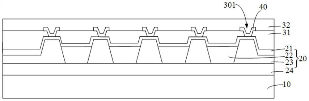
[0040] In addition, in the description of the present application, "plurality" means two or more, unless otherwise expressly and specifically defined. In this application, unless otherwise expressly specified and defined, a first feature "on" or "under" a second feature may include direct contact between the first and second features, or may include the first and second features Not directly but through additional features between them. Also...


PUM


Abstract

The invention provides a display panel, a manufacturing method of the display panel and a display device. The display panel comprises an array substrate; the pixel units are arranged on the array substrate in an array mode, and each pixel unit comprises a cathode layer; the first packaging layer is arranged on the cathode layer, the first packaging layer is provided with at least one groove, the groove is located between two adjacent pixel units, and the cathode layer is partially exposed out of the groove; and the auxiliary electrode layer is arranged on the first packaging layer and covers the cathode layer through the groove. The first packaging layer is provided with the groove, the groove is formed between the two adjacent pixel units, part of the cathode layer of each pixel unit is exposed out of the groove, the first packaging layer is provided with the auxiliary electrode layer, and the auxiliary electrode layer covers the cathode layer exposed out of the groove. Therefore, parallel connection between the auxiliary electrode layer and the cathode layer is realized, the resistance voltage drop of the cathode layer is reduced, and the display uniformity of the display panel is improved.

Description

technical field [0001] The present application relates to the technical field of display devices, and in particular, to a display panel, a method for manufacturing the display panel, and a display device. Background technique [0002] Compared with Liquid Crystal Display (LCD), Organic Light Emitting Diode (OLED) has the advantages of self-luminescence, wide viewing angle, lightness and so on, and is considered to be the next generation display technology. [0003] Among them, for top-emission OLED devices, a thin cathode is generally required to increase the transmittance of light, and the problems brought about by thin transparent cathodes are high resistance value and serious IR drop. It will cause the problem of uneven display. SUMMARY OF THE INVENTION [0004] The present application provides a display panel, a manufacturing method of the display panel, and a display device, so as to solve the problem of uneven display of the display panel. [0005] In one aspect, t...

Claims


Application Information

Patent Timeline
Patent Type & Authority Applications(China)
IPC IPC(8): H01L51/52H01L51/56H01L27/32
CPCH10K59/122H10K50/824H10K50/84H10K2102/3026H10K71/00
Inventor 胡泽虎
Owner SHENZHEN CHINA STAR OPTOELECTRONICS SEMICON DISPLAY TECH CO LTD
Why Eureka
Try Eureka