Chip packaging method, chip packaging body and electronic device

A chip packaging and electronic device technology, applied in circuits, electrical components, semiconductor devices, etc., can solve problems such as low bottom pad strength, structural reliability defects, and product welding pads falling off.

Pending Publication Date: 2022-07-01
SKY CHIP INTERCONNECTION TECH CO LTD
View PDF0 Cites 0 Cited by
  • Summary
  • Abstract
  • Description
  • Claims
  • Application Information

AI Technical Summary

Problems solved by technology

[0003] In the current solution, the chip is welded on the bottom pad, and the strength of the bottom pad is too low. There is a risk of the pad falling off when the product is soldered. As far as the current solution is concerned, there are certain defects in the structural reliability.

Method used


Image

  • Chip packaging method, chip packaging body and electronic device
  • Chip packaging method, chip packaging body and electronic device
  • Chip packaging method, chip packaging body and electronic device

Examples


Embodiment Construction

[0025] The technical solutions in the embodiments of the present application will be clearly and completely described below with reference to the drawings in the embodiments of the present application. Obviously, the described embodiments are only a part of the embodiments of the present application, but not all of the embodiments. Based on the embodiments in the present application, all other embodiments obtained by those of ordinary skill in the art without creative efforts shall fall within the protection scope of the present application.

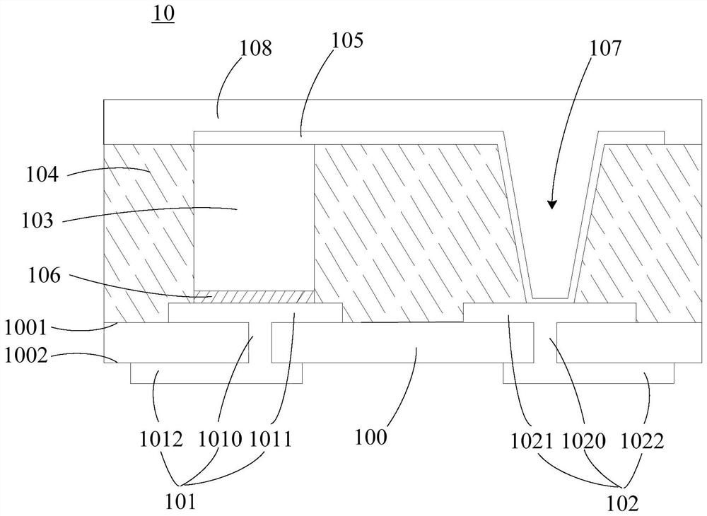
[0026] see figure 1 , figure 1It is a schematic cross-sectional structure diagram of an embodiment of the chip package of the present application. In this embodiment, the chip package 10 includes a carrier board 100 , a first pad 101 , a second pad 102 , a chip 103 , a first plastic encapsulation layer 104 and a metallization layer 105 . The carrier board 100 has opposite first surfaces 1001 and second surfaces 1002, and the carrier bo...


PUM


Abstract

The invention discloses a chip packaging method, a chip packaging body and an electronic device, and the method comprises the steps: providing a bearing plate which is provided with a first surface and a second surface which are opposite to each other; forming a first through hole and a second through hole in the bearing plate, and electroplating a metal layer to form a first bonding pad and a second bonding pad on the bearing plate; wherein the first bonding pad comprises a first connecting column, a first welding surface and a second welding surface which are used for filling the first through hole, the second bonding pad comprises a second connecting column, a third welding surface and a fourth welding surface which are used for filling the second through hole, and the first welding surface and the third welding surface are attached to the first surface of the bearing plate; the second welding surface and the fourth welding surface are attached to the second surface of the bearing plate; arranging a chip on the first bonding pad, and carrying out plastic package on the chip to form a first plastic package layer; and forming a metallization layer on one side, far away from the bearing plate, of the first plastic packaging layer so as to electrically connect the back surface of the chip with the second bonding pad. In this way, the welding reliability of products can be improved.

Description

technical field [0001] The present application relates to the technical field of chip packaging, and in particular, to a chip packaging method, a chip packaging body and an electronic device. Background technique [0002] As a kind of advanced packaging, FOPLP (fan-out board-level packaging) technology has been widely used in discrete devices. The fan-out board-level packaging area is smaller, and there is no substrate and interposer; The pin count density is also greater, which can better meet the end market's demand for chip miniaturization and high performance. [0003] In the current solution, the chip is soldered on the bottom pad, the strength of the bottom pad is too low, and there is a risk of the pad falling off when the product is soldered. As far as the current solution is concerned, there are certain defects in structural reliability. SUMMARY OF THE INVENTION [0004] The main technical problem to be solved by the present application is to provide a chip packa...

Claims


Application Information

Patent Timeline
Patent Type & Authority Applications(China)
IPC IPC(8): H01L21/48H01L21/50H01L21/56H01L23/498H01L23/31
CPCH01L21/4846H01L21/486H01L21/50H01L21/56H01L23/49805H01L23/49827H01L23/49838H01L23/3114H01L23/3121H01L23/3135H01L2224/18
Inventor 李俞虹
Owner SKY CHIP INTERCONNECTION TECH CO LTD
Why Eureka
Try Eureka