Thin imaging lens group and electronic equipment
An imaging lens, thin technology, applied in optical components, instruments, optics, etc., can solve the problems of poor imaging quality and low yield rate of three-chip lenses, achieve good correction of aberrations, reduce optical sensitivity, and improve imaging quality Effect
- Summary
- Abstract
- Description
- Claims
- Application Information
AI Technical Summary
Problems solved by technology
Method used
Image


Examples
Embodiment 1
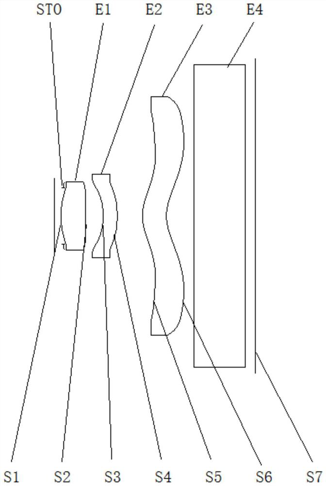
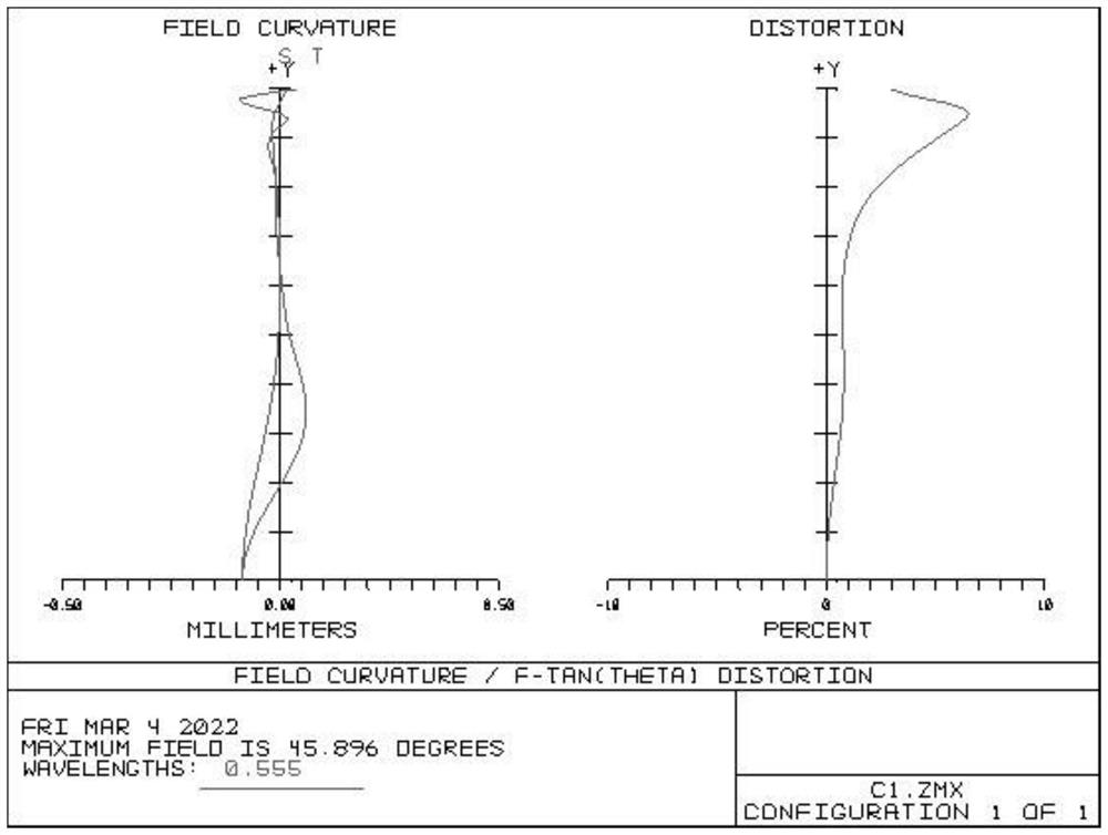
[0072] see Figure 1 to Figure 3 , figure 1 A schematic diagram of a thin imaging lens group according to Embodiment 1 of the present invention is shown, figure 2 From left to right are the astigmatism and distortion curves of a thin imaging lens group according to the first embodiment of the present invention, image 3 It is a spherical aberration curve diagram of a thin imaging lens group according to the first embodiment of the present invention.
[0073] This embodiment provides a thin imaging lens group, which includes a first lens E1 , a second lens E2 and a third lens E3 sequentially arranged from the object side to the image side.
[0074] Specifically, the first lens E1 has a positive refractive power, its object side S1 is convex at the paraxial position, and its image side S2 is concave at the paraxial position; the second lens E2 has a negative refractive power, and its object side S3 is at the paraxial position. The image side S4 is convex at the paraxial posi...
Embodiment 2
[0088] see Figure 4 to Figure 6 , Figure 4 A schematic diagram of a thin imaging lens group according to the second embodiment of the present invention is shown, Figure 5 From left to right are the astigmatism and distortion curves of a thin imaging lens group according to the second embodiment of the present invention, Image 6 It is a spherical aberration curve diagram of a thin imaging lens group according to the second embodiment of the present invention.
[0089] This embodiment provides a thin imaging lens group, which includes a first lens E1 , a second lens E2 and a third lens E3 sequentially arranged from the object side to the image side.
[0090] Specifically, the first lens E1 has positive refractive power, its object side S1 is convex at the paraxial position, and its image side S2 is convex at the paraxial position; the second lens E2 has negative refractive power, and its object side S3 is at the paraxial position. The image side S4 is convex at the paraxi...
Embodiment 3
[0099] see Figure 7 to Figure 9 , Figure 7 A schematic diagram of a thin imaging lens group according to Embodiment 3 of the present invention is shown, Figure 8 From left to right are the astigmatism and distortion curves of a thin imaging lens group according to the third embodiment of the present invention, Figure 9 It is a spherical aberration curve diagram of a thin imaging lens group according to the third embodiment of the present invention.
[0100] This embodiment provides a thin imaging lens group, which includes a first lens E1 , a second lens E2 and a third lens E3 sequentially arranged from the object side to the image side.
[0101] Specifically, the first lens E1 has positive refractive power, its object side S1 is convex at the paraxial position, and its image side S2 is convex at the paraxial position; the second lens E2 has negative refractive power, and its object side S3 is at the paraxial position. The image side S4 is convex at the paraxial positio...
PUM
 Abstract
Description
Claims
Application Information
 - Generate Ideas
- Intellectual Property
- Life Sciences
- Materials
- Tech Scout
- Unparalleled Data Quality
- Higher Quality Content
- 60% Fewer Hallucinations
Browse by: Latest US Patents, China's latest patents, Technical Efficacy Thesaurus, Application Domain, Technology Topic, Popular Technical Reports.
© 2025 PatSnap. All rights reserved.Legal|Privacy policy|Modern Slavery Act Transparency Statement|Sitemap|About US| Contact US: help@patsnap.com