Wafer transmission system and semiconductor equipment
A transmission system and semiconductor technology, applied in the field of semiconductor equipment, can solve problems such as chip loss or fragmentation, achieve the effects of avoiding chip loss or fragmentation, real-time and efficient detection, and improving reliability
- Summary
- Abstract
- Description
- Claims
- Application Information
AI Technical Summary
Problems solved by technology
Method used
Image

Examples
Embodiment 1
[0045] ginseng Figure 1 to Figure 11 The disclosed first embodiment of a wafer transfer system of the present invention.
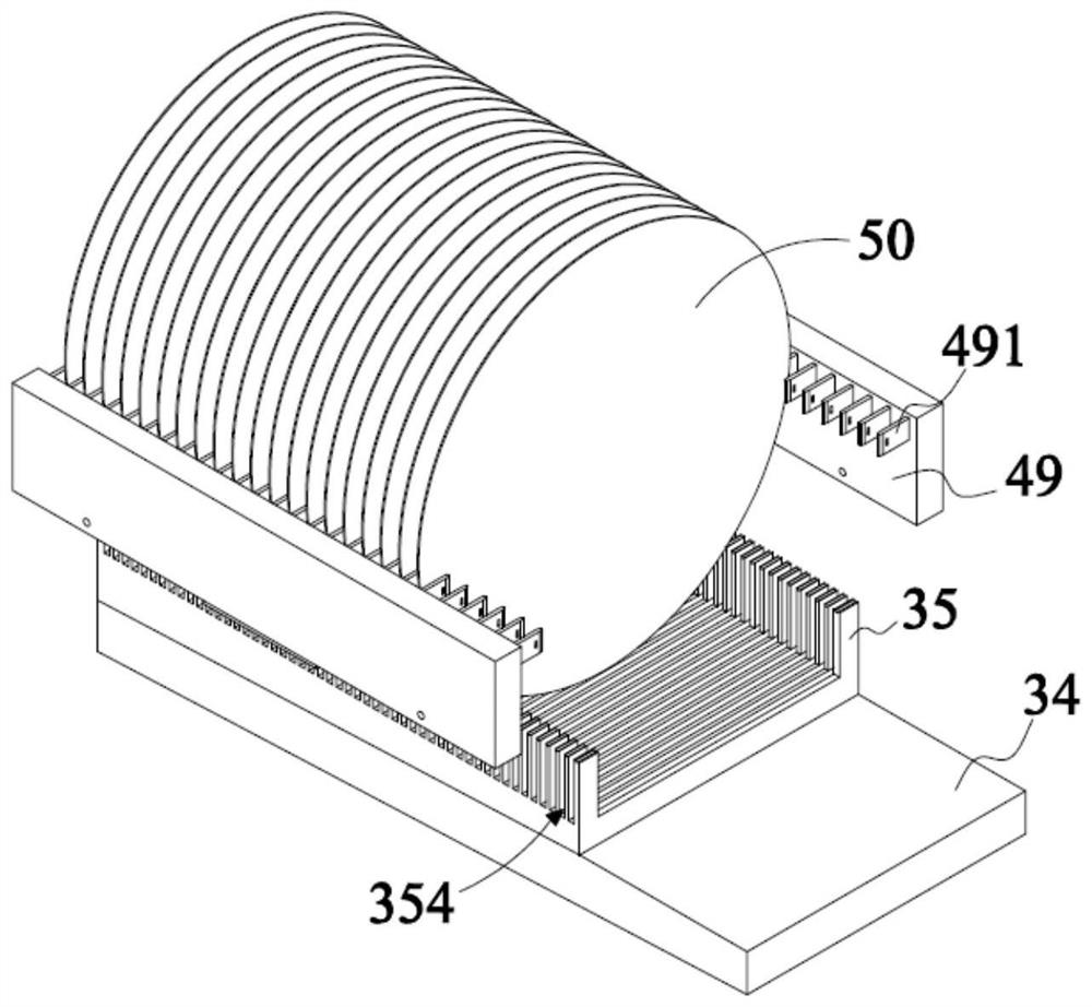
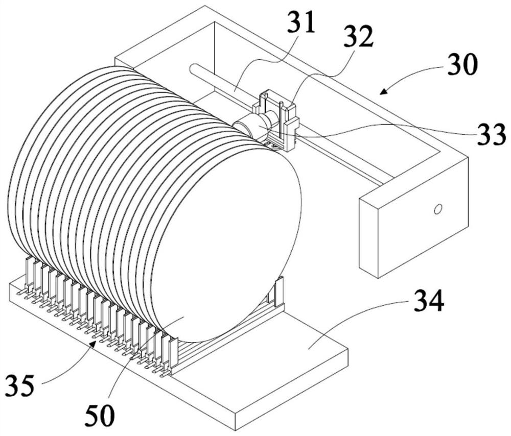
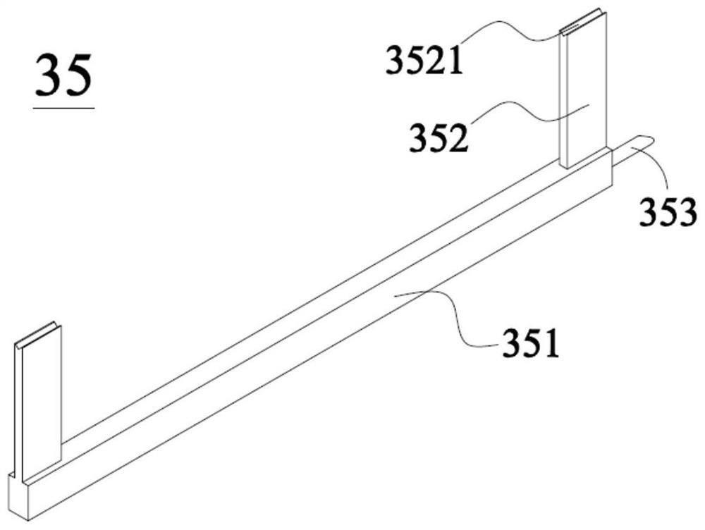
[0046]In this embodiment, a wafer transfer system includes: a buffer table 34 , a plurality of pressure detection units 35 arranged above the buffer table 34 for detecting the weight of the wafer, a photoelectric detection unit, and a pick-up unit. The pick-up unit includes two rotating grabbing plates 40 arranged in parallel. At least one side of the rotating grabbing plate 40 along its extension direction forms a fixed fork portion 42 supporting the edge of the wafer and having a first notch 420. Picking up The unit detects and sends the detection signal according to the photoelectric detection unit and the pressure detection unit to determine that the axial rotation angle of the rotary grabbing plate 40 is along the Figure 4 The rotation angle formed by the axis A turning in the direction shown by the arrow B. Preferably, the picking unit further in...
Embodiment 2
[0070] ginseng Figure 12 As shown, this embodiment discloses another specific implementation manner of a wafer transport system. The main difference between this embodiment and the wafer transfer system disclosed in Embodiment 1 is that in this embodiment, the pick-up unit includes two rows of movable forks arranged on the fixed forks, and the two rows of movable forks It is arranged on two opposite and different sides of the rotary grabbing plate 40 .
[0071] Specifically, in this embodiment, the movable fork 45a and the movable fork 43a are respectively located on two opposite sides of the substrate 41a, and the movable fork 45a and the movable fork can be driven according to the actual thickness data of the wafer 50. 43a is extended or retracted in the directions shown by arrow D and arrow D' respectively, so as to select the first notch 420 or the second notch 433 (or the second notch 453 ) of the opening size that best matches the thickness of the wafer 50 .
[0072]...
Embodiment 3
[0075] ginseng Figure 13 As shown, this embodiment discloses another specific implementation manner of a wafer transport system. The main difference between this embodiment and the wafer transfer system disclosed in Embodiment 2 is that in this embodiment, the pick-up unit includes a row of movable forks disposed on the fixed forks.
[0076] Specifically, in this embodiment, the movable forks 45a are respectively located on any side of the substrate 41b, and according to the actual thickness data of the wafer 50, the movable forks 45a can be driven to elongate in the direction shown by the arrow D or The first notch 420 or the second notch 433 that is retracted so as to select the opening size that best matches the thickness of the wafer 50 jointly supports the bottom edge of the wafer 50 to clamp and grasp the wafer 50 together.
[0077] The wafer transfer system shown in this embodiment has the same technical solutions as the wafer transfer system shown in Embodiment 1 and...
PUM
 Abstract
Description
Claims
Application Information
 - Generate Ideas
- Intellectual Property
- Life Sciences
- Materials
- Tech Scout
- Unparalleled Data Quality
- Higher Quality Content
- 60% Fewer Hallucinations
Browse by: Latest US Patents, China's latest patents, Technical Efficacy Thesaurus, Application Domain, Technology Topic, Popular Technical Reports.
© 2025 PatSnap. All rights reserved.Legal|Privacy policy|Modern Slavery Act Transparency Statement|Sitemap|About US| Contact US: help@patsnap.com