Parameter acquisition device, method, ion implantation method, and semiconductor process equipment

A parameter acquisition and ion beam technology, which is applied in semiconductor/solid-state device manufacturing, discharge tubes, electrical components, etc., can solve the problem of difficulty in real-time acquisition of current density, etc., so as to improve related calculation accuracy, improve efficiency and reliability, and improve monitoring. The effect of efficiency

Active Publication Date: 2022-08-05
GUANGZHOU CANSEMI TECH INC
View PDF9 Cites 0 Cited by
  • Summary
  • Abstract
  • Description
  • Claims
  • Application Information

AI Technical Summary

Problems solved by technology

[0004] In view of this, the present application provides a parameter acquisition device, method, ion implantation method and semiconductor process equipment to solve the problem that traditional ion implantation and other semiconductor process schemes are often difficult to obtain process-related parameters such as current density in real time

Method used


Image

  • Parameter acquisition device, method, ion implantation method, and semiconductor process equipment
  • Parameter acquisition device, method, ion implantation method, and semiconductor process equipment
  • Parameter acquisition device, method, ion implantation method, and semiconductor process equipment

Examples


Embodiment Construction

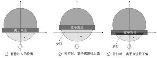
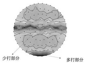
[0044] The inventors have researched semiconductor process schemes such as ion implantation, and found that when the ion beam is used for refilling of the wafer, if the position of the ion beam is readjusted, it is easy to change the relevant ion implantation parameters such as the ion position implanted into the wafer. It is also necessary to measure the process parameters such as the height of the ion beam, otherwise there may be problems such as figure 1 For the phenomenon shown, when the ion beam is deflected upward, some implant doses will be too low, resulting in the problem of undershooting in the corresponding area. When the ion beam is deflected downward, some implant doses will be too much, causing the corresponding area Multiple hits. like figure 2 As shown in the figure, the sheet resistance method can clearly characterize that in the corresponding wafer, there are problems such as unevenness in the over-dosing portion corresponding to the excessively large impla...


PUM


Abstract

The present application discloses a parameter acquisition device, method, ion implantation method and semiconductor process equipment. The parameter acquisition device includes: a baffle, a Faraday cup and a current detection device, the baffle includes a slit; the baffle is arranged between the ion beam source that generates the ion beam current and the Faraday cup, and is configured to moving perpendicular to the height of the Faraday cup and blocking the ion beam current, the slit for passing a portion of the ion beam current; the Faraday cup is configured to generate a current when receiving the ion beam current ; The current detection device is configured to detect the magnitude of the current of the Faraday cup, where the magnitude of the current is used to characterize the current density corresponding to the Faraday cup. The present application can quickly and accurately obtain the current density corresponding to the Faraday cup, thereby obtaining relevant process parameters.

Description

technical field [0001] The present application relates to the field of semiconductor technology, and in particular, to a parameter acquisition device, method, ion implantation method, and semiconductor process equipment. Background technique [0002] With the development of semiconductor technology to large scale integration (LSI) or very large scale integration (VLSI), the size of semiconductor devices is getting smaller and smaller, and the requirements for ion implantation and other processes are also getting higher and higher. As an example, the Implant machine is mainly a machine that injects a specific energy, ion mass, and specific angle into the wafer to form a PN junction; this type of machine has very strict dose requirements in the process of ion implantation. Generally, The dose error is required to be no more than 3%, and if the dose is too large or too small, the wafer will be scrapped. [0003] During the ion implantation process, due to the voltage jump (Gli...

Claims


Application Information

Patent Timeline
Patent Type & Authority Patents(China)
IPC IPC(8): H01J37/244H01J37/304H01J37/317H01L21/67
CPCH01J37/244H01J37/3171H01J37/304H01L21/67253
Inventor 陶卓朱红波
Owner GUANGZHOU CANSEMI TECH INC
Why Eureka
Try Eureka