Display panel and mobile terminal
A technology for display panels and substrates, which is applied to electrical components, electric solid devices, circuits, etc., and can solve problems such as viewing angle differences of display panels
- Summary
- Abstract
- Description
- Claims
- Application Information
AI Technical Summary
Problems solved by technology
Method used
Image
Examples
Embodiment 1
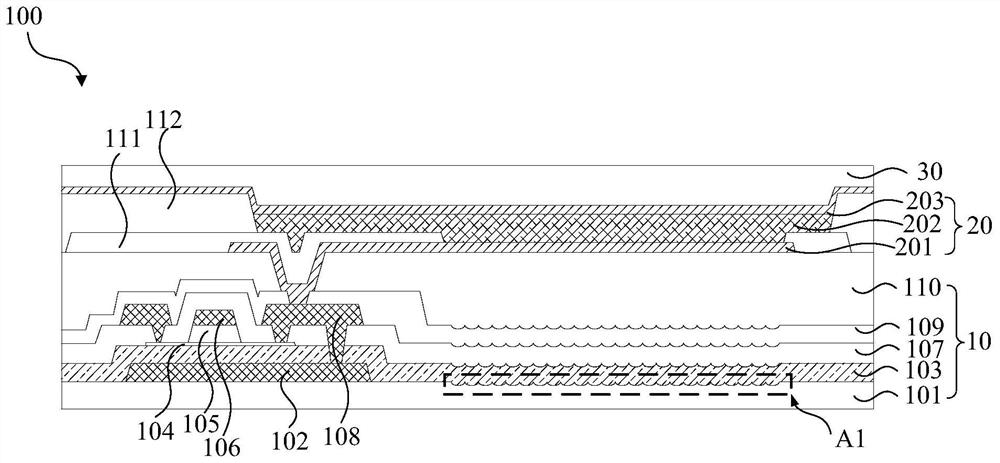
[0038] like figure 1 As shown, it is a cross-sectional structure diagram of the display panel 100 provided in the first embodiment of the present application; wherein, the display panel 100 provided in this embodiment includes an array structure layer 10, and the light-emitting devices disposed on the array structure layer 10 20 and an encapsulation layer 30 disposed on the light emitting device 20 .
[0039] In the embodiment of the present application, the array structure layer 10 includes a first substrate 101, a light shielding layer 102 disposed on the first substrate 101, disposed on the first substrate 101 and completely covering the light shielding layer 102 The buffer layer 103, the active layer 104 disposed on the buffer layer 103, the gate insulating layer 105 disposed on the active layer 104, the gate metal layer disposed on the gate insulating layer 105 106. The interlayer insulating layer 107 disposed on the buffer layer 103 and completely covering the active la...
Embodiment 2
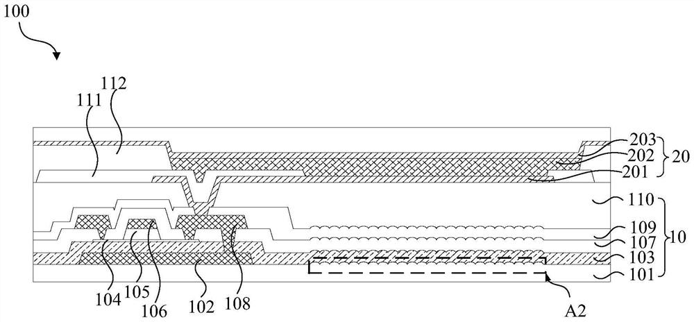
[0064] like image 3 As shown, it is a cross-sectional structure diagram of the display panel 100 provided in the second embodiment of the present application; Figure 4 The display panel provided for the second embodiment of the present application corresponds to image 3 The enlarged schematic diagram at A2 in ; Figure 4 as well as image 3 It can be seen that the structure of the display panel 100 in the second embodiment of the present application is mostly the same as the structure of the first embodiment of the present application, the only difference is that the surface of the first substrate 101 close to the buffer layer 103 is provided with multiple layers. a plurality of second protrusions 1012, the surface of the buffer layer 103 close to the first substrate 101 is provided with a plurality of second grooves 1032, and each of the second protrusions 1012 is connected to each of the first substrate 101. The two grooves 1032 are arranged correspondingly;
[0065]W...
Embodiment 3
[0078] like Figure 5 As shown, it is a cross-sectional structure diagram of the display panel 100 provided in the third embodiment of the present application; wherein, the structure of the display panel 100 in the third embodiment of the present application is mostly the same as the structure of the first embodiment of the present application, the only difference is that , the substrate includes a second substrate 501 and a third substrate 502, the light emitting device 20 is disposed on the second substrate 501, the encapsulation layer 30 is disposed on the light emitting device 20, and the third substrate 502 set on the encapsulation layer 30;
[0079] Wherein, the encapsulation layer 30 is provided with a plurality of the grooves, the surface of the third substrate 502 close to the encapsulation layer 30 is provided with a plurality of the protrusions, each of the grooves corresponds to a the bump.
[0080] In the embodiment of the present application, the first refracti...
PUM
 Abstract
Description
Claims
Application Information
 - Generate Ideas
- Intellectual Property
- Life Sciences
- Materials
- Tech Scout
- Unparalleled Data Quality
- Higher Quality Content
- 60% Fewer Hallucinations
Browse by: Latest US Patents, China's latest patents, Technical Efficacy Thesaurus, Application Domain, Technology Topic, Popular Technical Reports.
© 2025 PatSnap. All rights reserved.Legal|Privacy policy|Modern Slavery Act Transparency Statement|Sitemap|About US| Contact US: help@patsnap.com


