Three-dimensional structure electronic device, manufacturing method and device

A technology of electronic devices and three-dimensional structures, which is applied to the device for coating liquid on the surface, additive manufacturing, coating, etc., can solve the problems of three-dimensional devices that cannot meet the requirements of functional and structural integration, and achieve efficient, fast and cost-saving manufacturing processes Effect

Pending Publication Date: 2022-03-25
杭州华遨科技有限公司
View PDF0 Cites 0 Cited by
  • Summary
  • Abstract
  • Description
  • Claims
  • Application Information

AI Technical Summary

Problems solved by technology

[0003] Based on this, it is necessary to provide a three-dimensional structure electronic device, manufacturing method and device for the problem that the existing technology cannot meet the problem of three-dimensional device manufacturing with functional structure integration

Method used


Image

  • Three-dimensional structure electronic device, manufacturing method and device
  • Three-dimensional structure electronic device, manufacturing method and device
  • Three-dimensional structure electronic device, manufacturing method and device

Examples


Embodiment Construction

[0033] The present invention can be implemented in many ways other than those described here, and those skilled in the art can make similar improvements without departing from the connotation of the present invention, so the present invention is not limited by the specific embodiments disclosed below.

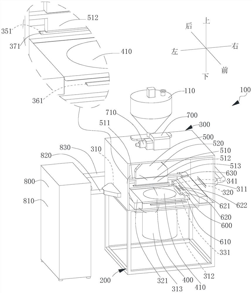
[0034] In the description of the present invention, the terms "front", "rear", "upper", "lower", "left", "right", "center", "longitudinal", "transverse", "length" are used The orientation or positional relationship indicated by etc. is based on the orientation or positional relationship shown in the drawings, and is only for the convenience of describing the present invention and simplifying the description. The fact that a first feature is "on" or "under" a second feature may mean that the first and second features are in direct contact, or that the first and second features are in indirect contact through an intermediary. The terms "first" and "second" are used for descriptiv...


PUM


Abstract

The invention relates to a three-dimensional structure electronic device and a manufacturing method and device, and the method comprises the following steps: S1, designing a three-dimensional model of the three-dimensional structure electronic device, and reserving a via hole position; s2, performing layering processing on the three-dimensional model; s3, the mixed slurry is laid on a workbench and cured to form a first base body layer, and a first conductor layer comprises a radiation structure formed at the position of the via hole; s4, spraying a binding agent on the first matrix layer to form a first binding layer; s5, spraying conductive slurry on the first bonding layer to form a first conductor layer; s6, spraying a binding agent on the first conductor layer to form a second binding layer; and S7, the steps S3-S6 are repeatedly executed until the nth conductor layer and the (n + 1) th substrate layer are completed, and the three-dimensional structure electronic device is obtained. And S8, cleaning the three-dimensional structure electronic device, and bending the radiation structure at the position of the via hole. By controlling the technological process, manufacturing of the structure-function integrated three-dimensional structure electronic device is achieved, and interconnection between conductor layers can be achieved without independently plating copper in the via hole.

Description

technical field [0001] The invention relates to the technical field of structural electronic circuits, in particular to three-dimensional structural electronic devices, manufacturing methods and devices. Background technique [0002] With the increasing complexity and rich functions of modern electronic systems, new functional-structural three-dimensional circuits based on the integration of electronic circuits and functional structures are increasingly widely used. Different from traditional electronic circuit devices, three-dimensional circuits usually need to integrate various components such as sensor elements, actuators, control circuits, communication antennas and energy supply units in an extremely compact space. The space for accommodating electronic circuits is extremely limited. This makes the circuit board based on plane printing unable to meet the requirements of the three-dimensional circuit. The current methods used to manufacture three-dimensional circuits ca...

Claims


Application Information

Patent Timeline
IPC IPC(8): B22F12/53B22F12/30B22F5/00B22F10/28B33Y30/00B33Y10/00B33Y80/00B05C5/02B05C11/10B05D7/24
CPCB22F12/53B22F12/30B22F5/00B22F10/28B33Y30/00B33Y10/00B33Y80/00B05C5/0208B05C11/10B05D7/24Y02P10/25
Inventor 俞红祥王康恒
Owner 杭州华遨科技有限公司
Why Eureka
Try Eureka