Testing device

A technology for testing equipment and tested parts, which is applied in the direction of measuring equipment, single semiconductor device testing, and electrical measurement, and can solve problems such as unsatisfactory actual needs and complex circuit structures.

Pending Publication Date: 2022-03-22
河北博威集成电路有限公司
View PDF0 Cites 0 Cited by
  • Summary
  • Abstract
  • Description
  • Claims
  • Application Information

AI Technical Summary

Problems solved by technology

[0004] The embodiment of the present invention provides a test device to solve the problem that the circuit structure in the prior art is complex and cannot meet the actual needs

Method used


Image

  • Testing device
  • Testing device
  • Testing device

Examples


Embodiment Construction

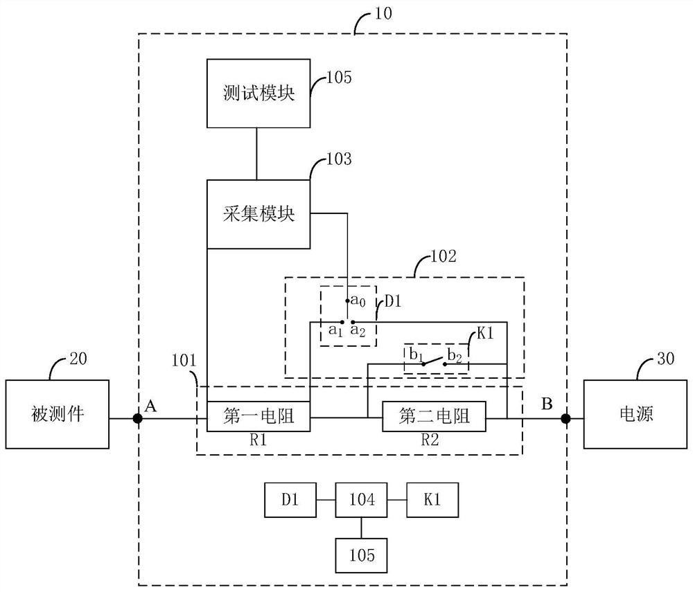
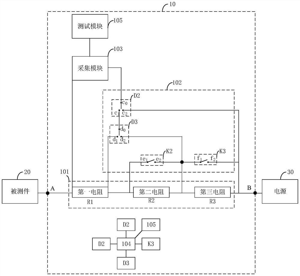
[0044] In order to enable those skilled in the art to better understand this solution, the technical solution in this solution embodiment will be clearly described below in conjunction with the accompanying drawings in this solution embodiment. Obviously, the described embodiment is a part of this solution Examples, but not all examples. Based on the embodiments in this solution, all other embodiments obtained by persons of ordinary skill in the art without creative efforts shall fall within the protection scope of this solution.

[0045]The term "comprising" and any other variants in the description and claims of this solution and the above drawings mean "including but not limited to", and are intended to cover non-exclusive inclusion and are not limited to the examples listed herein. In addition, the terms "first" and "second", etc. are used to distinguish different objects, not to describe a specific order.

[0046] The realization of the present invention is described in ...


PUM


Abstract

The invention provides a testing device. The testing device comprises a first interface and a second interface; the first interface is used for connecting a tested piece; the second interface is used for connecting an external power supply; the testing device further comprises a resistor module, a switch module, an acquisition module, a control module and a testing module. The test module is used for generating a control instruction according to the current working state of the tested piece and sending the control instruction to the control module; the control module is used for controlling the state of the switch module according to the control instruction, so that the resistor module, the switch module and the acquisition module form a working loop corresponding to the current working state of the tested piece; the acquisition module is used for acquiring electrical parameters of the resistor module in the working loop; and the test module is also used for acquiring the electrical parameters, acquired by the acquisition module, of the resistor module in the working loop, and calculating the output electrical parameters of the tested piece according to the electrical parameters. According to the invention, the test reliability can be improved.

Description

technical field [0001] The invention relates to the technical field of electrical parameter acquisition, in particular to a testing device. Background technique [0002] Semiconductor device testing is an important means to ensure that product performance meets the requirements of relevant indicators and reduce product failure rates. The efficient and accurate collection of performance indicators of semiconductor devices places extremely high requirements on test equipment and test methods. Semiconductor devices have multiple product test states such as pinch-off, static, and saturation, and the current levels to be collected under different states are very different. In the pinch-off and static state, the minimum current level to be accurately collected is at the uA level, and the highest is at the hundreds of mA level; in the saturated state, the minimum current level to be accurately collected is at the ten-uA level, and the highest is at the 10A level or even higher. T...

Claims


Application Information

Patent Timeline
Patent Type & Authority Applications(China)
IPC IPC(8): G01R31/26
CPCG01R31/2607
Inventor 段磊李浩张博郭跃伟黎荣林崔健
Owner 河北博威集成电路有限公司
Why Eureka
Try Eureka