
Self-adaptive photoelectric interface device, FPGA and method

A photoelectric interface and self-adaptive technology, applied in the field of communication, can solve the problems of increasing the number of cabinets used in the area occupied by the communication room, the overall replacement of router equipment, and the high cost of router equipment, so as to improve the summarization and calculation speed, reduce equipment costs, and reduce costs. Effect

Pending Publication Date: 2022-02-11
BEIJING SIFANG JIBAO ENG TECH +1
View PDF0 Cites 0 Cited by
  • Summary
  • Abstract
  • Description
  • Claims
  • Application Information

AI Technical Summary

Problems solved by technology

This correspondingly increases the number of cabinets used and the occupied area of ​​the communication room
[0006] Second, since each COMBO communication interface needs to have an optical port slot and an electrical port slot, for a platform with a large number of data information collection points, the double redundancy of the number of slots leads to equipment cost a substantial increase in
Therefore, not only the cost of router equipment with COMBO communication interface is relatively high, but also the cost of realizing application platform construction is also greatly increased
[0007] Third, due to the fact that there are a large number of redundant communication interfaces in the system that cannot be effectively connected, the long-term idleness of the communication slots will also cause various unexpected failures in the communication equipment interfaces, and when the data information collection point access mode When a change occurs, the redundant communication interface may not be able to work effectively, which leads to the occurrence of problems such as the overall replacement of router equipment

Method used


Image

  • Self-adaptive photoelectric interface device, FPGA and method
  • Self-adaptive photoelectric interface device, FPGA and method
  • Self-adaptive photoelectric interface device, FPGA and method

Examples


Embodiment Construction

[0034] The application will be further described below in conjunction with the accompanying drawings. The following examples are only used to illustrate the technical solutions of the present invention more clearly, but not to limit the protection scope of the present application.

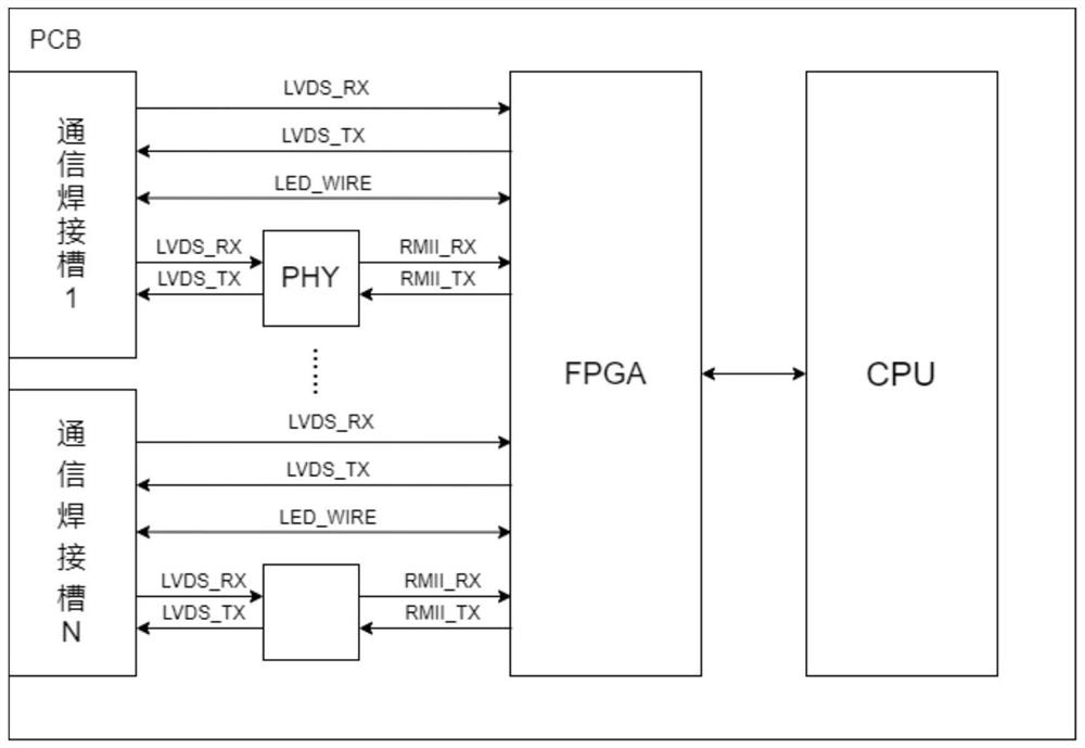
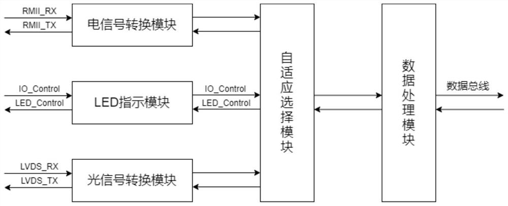
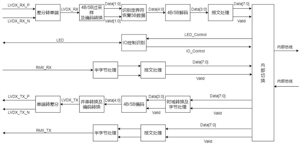
[0035] figure 1 It is a schematic diagram of the internal structure of an adaptive photoelectric interface device of the present invention. Such as figure 1As shown, the first aspect of the present invention relates to a device for an adaptive photoelectric interface, wherein the device includes a PCB circuit board disposed inside the device, and a plurality of communication welding slots connected to the PCB circuit board and disposed on the device housing ; One or more of the communication welding slots are used to weld the RJ45 socket and the PHY chip to realize the input and output of electrical signals through the RJ45 interface; or, one or more of the communication welding slots are used to...


PUM


Abstract

The invention relates to a self-adaptive photoelectric interface device, which is characterized by comprising a PCB arranged in the device and a plurality of communication welding grooves connected with the PCB and arranged on a device shell, one or more communication welding grooves are used for welding a RJ45 slot and a PHY chip so as to realize input and output of electric signals through a RJ45 interface; or one or more of the communication welding grooves are used for welding SFP slots, so that the input and output of optical signals are realized through a SFP transceiver. The device and the method are convenient to implement and low in cost, and the equipment can be updated at the minimum cost at any time.

Description

technical field [0001] The present invention relates to the communication field, and more specifically, relates to a device, an FPGA and a method for an adaptive photoelectric interface. Background technique [0002] At present, in the fields of power system and industrial control, there are a large number of data information collection points on various application platforms. Due to the different working conditions, distances, environments and other indicators of the data information collection points, as well as the continuous improvement of the integration and complexity of various application platforms, some of the data information from the data information collection points are transmitted through Ethernet dual The twisted wire transmission method realizes the data transmission to the main control unit in the platform, and the other part adopts the optical fiber transmission method to realize the data transmission. In other words, the data information transmitted throu...

Claims


Application Information

Patent Timeline
IPC IPC(8): H04L49/111H04L69/321
CPCH04L69/321
Inventor 孟凡虎胡炯周涛杨海池李新华戴展波蒋新成陈楠
Owner BEIJING SIFANG JIBAO ENG TECH
Learn More