R-type non-contact loading PCB combined jig

A combined fixture and non-contact technology, which is applied in the direction of packaging, transportation and packaging, and containers to prevent mechanical damage, etc., can solve the problems of PCB board friction, poor PCB fixing stability, and easily damaged printed circuits, etc., to achieve quick disassembly The effect of installation and combination, fixed and stable, and convenient maintenance

Pending Publication Date: 2022-01-18
广东智联半导体装备有限公司
View PDF1 Cites 1 Cited by
  • Summary
  • Abstract
  • Description
  • Claims
  • Application Information

AI Technical Summary

Problems solved by technology

[0003] When the PCB is reprinted, it is stacked and transported by stacking, but under the action of gravity, the horizontal fixture will cause the middle of the PCB board to contact each other, causing the PCB to rub against each other, such as high-end HDI, MSAP, and IC carrier boards. The circuit of the PCB board is very thin, which makes it easy to damage the printed circuit during handling or manual operation, and the fixation stability of the PCB is poor, and it is inconvenient to use. The Chinese patent discloses a circuit board storage rack. (Authorized announcement number CN203419420U) , this patented technology can effectively prevent the surface of the circuit board from being scratched or scratched, but it cannot solve the friction between PCB boards placed on the same storage layer; and if it is set at an angle, there will be a triangular gap in the upper part, and the space utilization rate is low; There are no limit and protective structures at the front and rear ends of the PCB, resulting in the risk of bumping and falling out of the front and rear ends of the PCB

Method used


Image

  • R-type non-contact loading PCB combined jig
  • R-type non-contact loading PCB combined jig
  • R-type non-contact loading PCB combined jig

Examples


Embodiment Construction

[0026] The present invention will be further described in detail below in conjunction with the accompanying drawings and specific embodiments. The embodiments of the present invention have been presented for purposes of illustration and description, but are not intended to be exhaustive or to limit the invention to the form disclosed. Many modifications and changes will be apparent to those of ordinary skill in the art. The embodiment was chosen and described in order to better explain the principles of the invention and the practical application, and to enable others of ordinary skill in the art to understand the invention and design various embodiments with various modifications as are suited to the particular use.

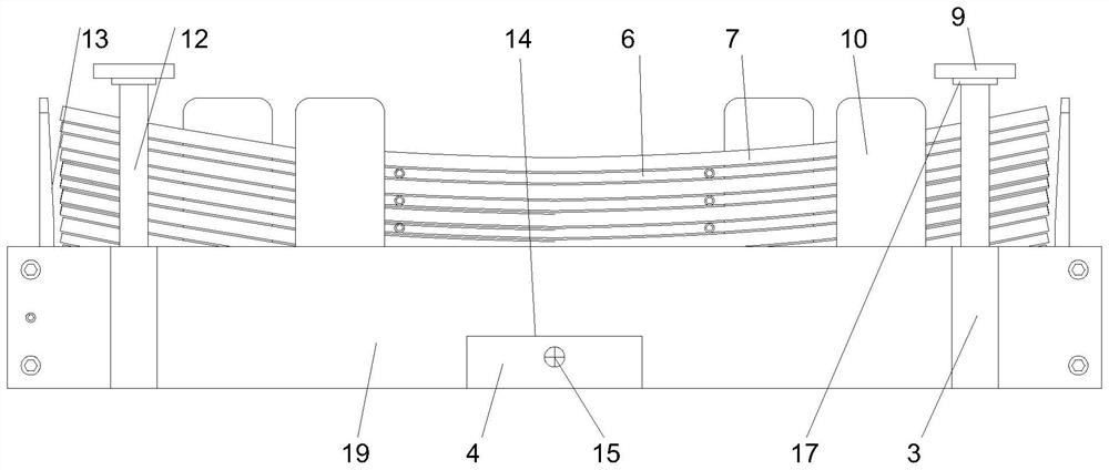
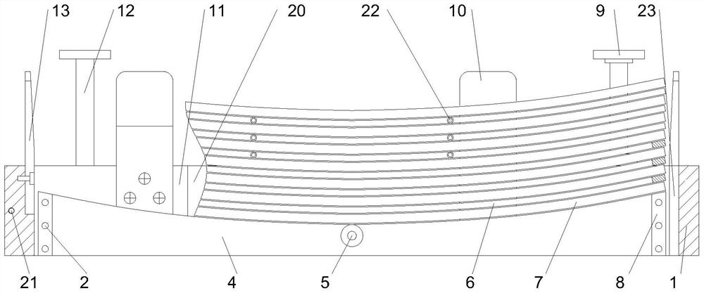
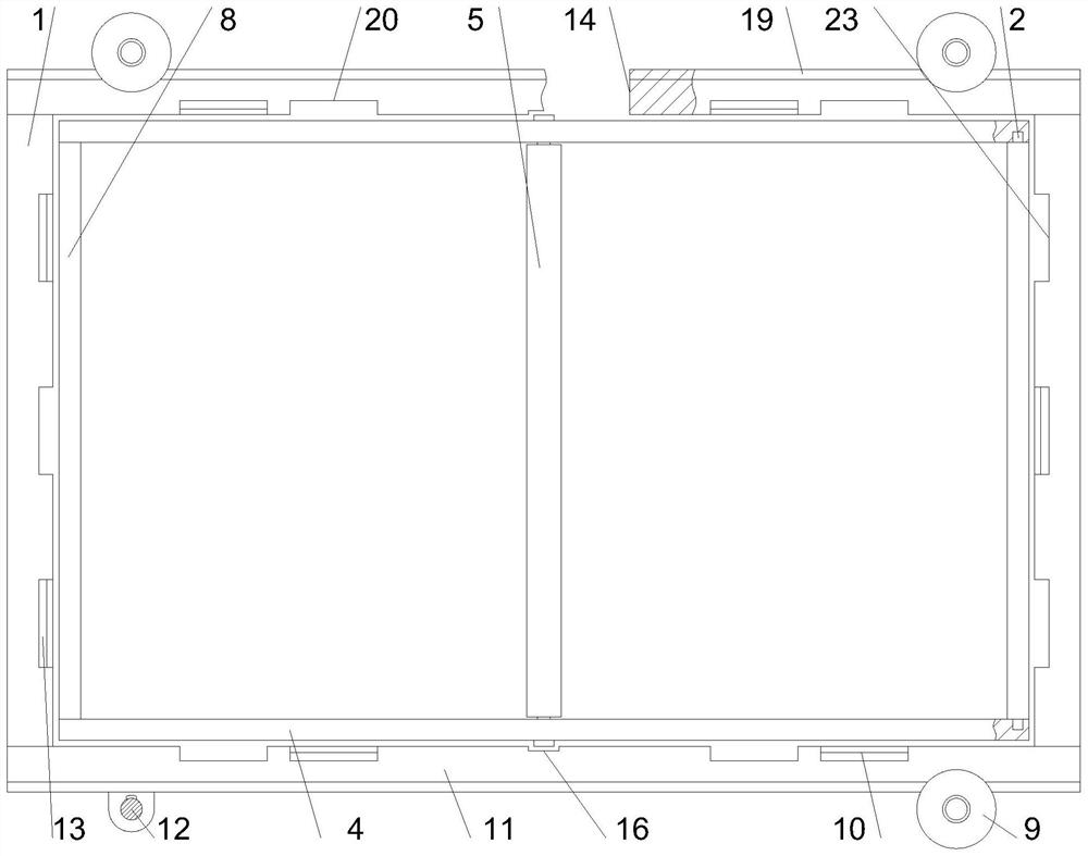
[0027] see Figure 1-8 In this embodiment, an R-type non-contact loading PCB combination fixture is provided, including a first outer plate 1, an inner frame, a second outer plate 11, a slide bar 12, a bulkhead, a relay bar and a synchronous bar, two A second ...


PUM


Abstract

The invention discloses a R-type non-contact loading PCB combined jig comprising first outer plates, an inner frame, second outer plates, sliding rods, partition frames, relay rods and synchronizing rods, wherein the second outer plates are connected between the front ends and the rear ends of the two first outer plates in a pressing mode, and pressing plates are installed on the outer walls of the ends, away from the first outer plates, of the second outer plates in a covering mode. The top ends of a first inner plate and a second inner plate are provided with the continuous arc-shaped grooves, and the lowest point of the corresponding arc-shaped groove is located in the middle of the top end of the first inner plate; a PCB can be changed into an arc shape depending on self toughness through the arc shape, and the PCB is fixed by pressing the periphery in cooperation with stacked spacers; and non-contact of each layer of PCB is truly achieved.

Description

technical field [0001] The invention relates to the field of PCB jigs, in particular to an R-type non-contact loading PCB combination jig. Background technique [0002] PCB, the Chinese name is printed circuit board, also known as printed circuit board, is an important electronic component, a support for electronic components, and a carrier for electrical connections of electronic components. Because it is made using electronic printing, it is called a "printed" circuit board. [0003] When the PCB is reprinted, it is stacked and transported by stacking, but under the action of gravity, the horizontal fixture will cause the middle of the PCB board to contact each other, causing the PCB to rub against each other, such as high-end HDI, MSAP, and IC carrier boards. The circuit of the PCB board is very thin, which makes it easy to damage the printed circuit during handling or manual operation, and the fixation stability of the PCB is poor, and it is inconvenient to use. The Chi...

Claims


Application Information

Patent Timeline
Patent Type & Authority Applications(China)
IPC IPC(8): B65D25/02B65D25/10B65D81/05B65D85/62
CPCB65D25/02B65D25/10B65D81/05B65D85/62
Inventor 戴泳崇侯宣来李冬林王诚
Owner 广东智联半导体装备有限公司
Why Eureka
Try Eureka