System and method for wafer de-bonding

A debonding and wafer technology, applied in the field of wafer debonding system, can solve problems such as wafer cracking, achieve easy assembly, improve output yield, and solve the effects of wafer cracking

Pending Publication Date: 2021-12-31
华芯半导体研究院(北京)有限公司 +1
View PDF0 Cites 0 Cited by
  • Summary
  • Abstract
  • Description
  • Claims
  • Application Information

AI Technical Summary

Problems solved by technology

The system is simple in structure, easy to assemble and disassemble, and has a wide range of applications. It can be temporarily installed and disassembled in the normal wet machine slot; and in the wet debonding system, the use of external force is avoided, which solves the problem of machine chuck adsorption and push back Problems such as wafer cracks caused by uneven output during the chip debonding process, thereby reducing the number of defective chips and improving the output yield

Method used


Image

  • System and method for wafer de-bonding
  • System and method for wafer de-bonding
  • System and method for wafer de-bonding

Examples


Embodiment Construction

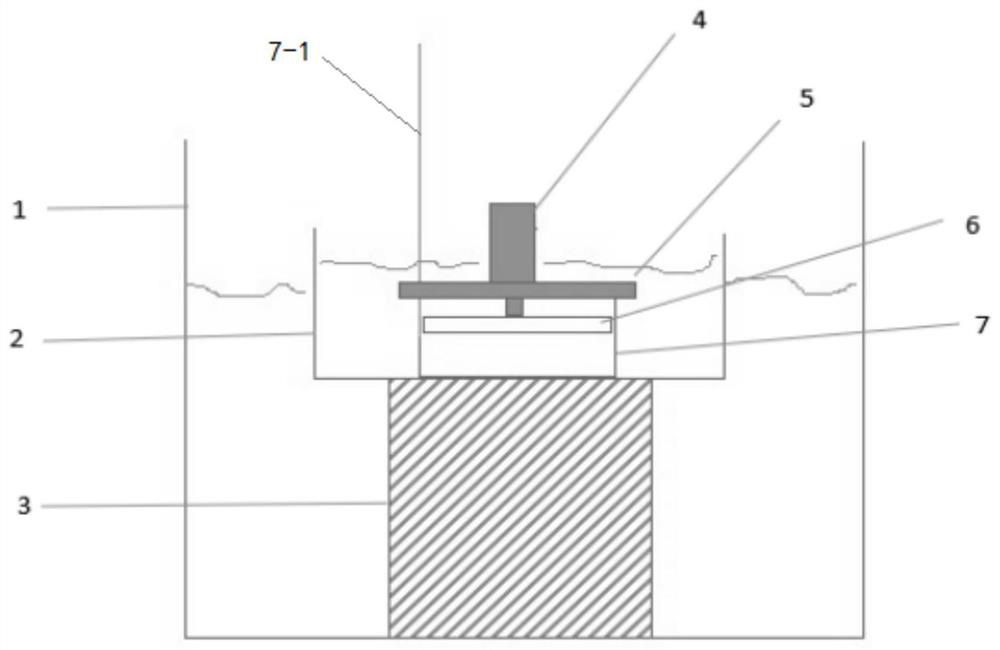
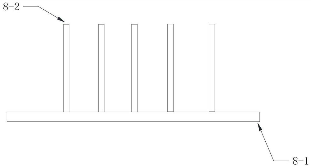
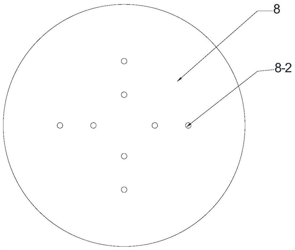
[0032] Embodiments of the invention are described in detail below, examples of which are illustrated in the accompanying drawings. The embodiments described below by referring to the figures are exemplary and are intended to explain the present invention and should not be construed as limiting the present invention.

[0033] In describing the present invention, it should be understood that the terms "center", "longitudinal", "transverse", "length", "width", "thickness", "upper", "lower", "front", " Rear", "Left", "Right", "Vertical", "Horizontal", "Top", "Bottom", "Inner", "Outer", "Axial", "Radial", "Circumferential" The orientation or positional relationship indicated by etc. is based on the orientation or positional relationship shown in the drawings, and is only for the convenience of describing the present invention and simplifying the description, rather than indicating or implying that the referred device or element must have a specific orientation, use a specific Azim...


PUM


Abstract

The invention discloses a system and method for wafer de-bonding. The system comprises a heating bath, a support, a de-bonding liquid tank, a wafer container and a connecting rod, wherein the heating bath is used for containing a water bath or an oil bath; the support is arranged in the heating bath; the de-bonding liquid tank is arranged on the support, and the de-bonding liquid tank is used for containing a de-bonding liquid; the wafer container is used for containing a wafer to be de-bonded, the wafer container is movable, and a plurality of holes are formed in the bottom wall and at least part of the side wall of the wafer container; and the connecting rod is used for fixing a ceramic plate of the wafer to be de-bonded. The system is simple in structure, easy to assemble and disassemble and wide in application, and can be temporarily assembled and disassembled in a normal wet process machine table slot; and in the wet de-bonding system, external force is avoided, and the problems of dark crack of the wafer and the like caused by non-uniform force output in the wafer pushing and de-bonding process after the chuck adsorption of the machine table are solved, so that the number of defective wafers is reduced, and the yield is improved.

Description

technical field [0001] The present invention relates to the field of chip technology, in particular, the present invention relates to a system and method for wafer debonding. Background technique [0002] After thinning and polishing, the VCSEL device process needs to debond the wafer (wafer) bonded to the ceramic disk. At present, the commonly used debonding methods are mainly divided into two types: debonding after the chuck is adsorbed, and debonding by wet soaking. When the chuck is adsorbed by the machine and the chip is pushed out for debonding, problems such as thin wafer thickness, uneven output, and dark cracking of the wafer are often encountered, resulting in a high fragmentation rate of the wafer. However, there is no mature automatic machine for wet soaking and debonding, and the fragmentation rate of manual chip removal is relatively high. Contents of the invention [0003] The present invention aims to solve one of the technical problems in the related art...

Claims


Application Information

Patent Timeline
Patent Type & Authority Applications(China)
IPC IPC(8): H01L21/67
CPCH01L21/67086H01L21/67017
Inventor 韩浩江蔼庭王青王健军吴敦文
Owner 华芯半导体研究院(北京)有限公司
Why Eureka
Try Eureka