Pixel arrangement structure, metal mask plate and organic light-emitting display device
A metal mask and pixel arrangement technology, which is applied in metal material coating process, vacuum evaporation plating, coating, etc., can solve the problems such as difficulty in improving display brightness and service life, and achieve improved display brightness and service life, The effect of enhancing the strength and increasing the pixel aperture ratio
- Summary
- Abstract
- Description
- Claims
- Application Information
AI Technical Summary
Problems solved by technology
Method used
Image

Examples
Embodiment 1
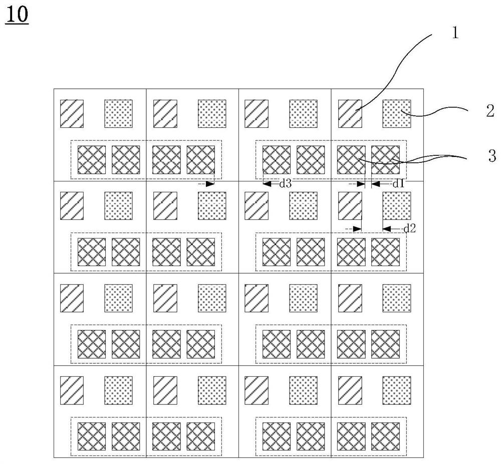
[0054] Please refer to figure 1 , which is a schematic structural diagram of a pixel arrangement structure according to Embodiment 1 of the present invention. Such as figure 1 As shown, the pixel arrangement structure 10 includes: a plurality of pixel units (not shown in the figure), the plurality of pixel units are arranged in an array in sequence, and each pixel unit (shown in a single solid line box) includes A first sub-pixel 1, a second sub-pixel 2, and two third sub-pixels 3 with equal areas, the two third sub-pixels 3 with equal areas are arranged in the same row and have a first distance d1, the The first sub-pixel 1 and the second sub-pixel 2 are arranged in another adjacent row and have a second distance d2; wherein, the first distance d1 is smaller than the second distance d2, and the two equal-area The vertical line of the center connection line of the third sub-pixel 3 does not overlap with the vertical center line of the pixel unit, and in two laterally adjacen...
Embodiment 2
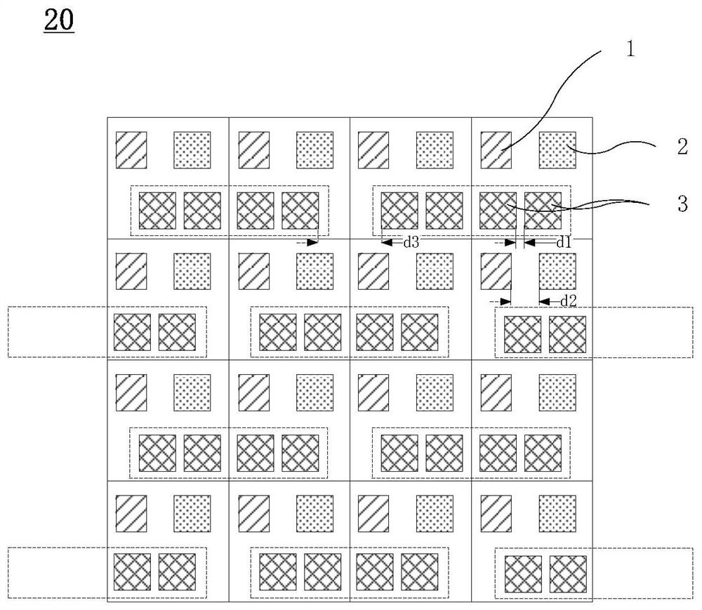
[0080] Please refer to image 3 , which is a schematic structural diagram of a pixel arrangement structure according to Embodiment 2 of the present invention. Such as image 3 As shown, the pixel arrangement structure 20 includes: a plurality of pixel units (not shown in the figure), the plurality of pixel units are arranged in an array in sequence, and each pixel unit (shown in a single solid line box) includes A first sub-pixel 1, a second sub-pixel 2, and two third sub-pixels 3 with equal areas, the two third sub-pixels 3 with equal areas are arranged in the same row and have a first distance d1, the The first sub-pixel 1 and the second sub-pixel 2 are arranged in another adjacent row and have a second distance d2; wherein, the first distance d1 is smaller than the second distance d2, and the two equal-area The vertical line of the center connection line of the third sub-pixel 3 does not overlap with the vertical center line of the pixel unit, and in two laterally adjacen...
Embodiment 3
[0101] Please refer to Figure 7 , which is a schematic structural diagram of a pixel arrangement structure according to Embodiment 3 of the present invention. Such as Figure 7As shown, the pixel arrangement structure 30 includes: a plurality of pixel units (not shown in the figure), the plurality of pixel units are arranged in an array in sequence, and each pixel unit (shown in a single solid line box) includes A first sub-pixel 1, a second sub-pixel 2, and two third sub-pixels 3 with equal areas, the two third sub-pixels 3 with equal areas are arranged in the same row and have a first distance d1, the The first sub-pixel 1 and the second sub-pixel 2 are arranged in another adjacent row and have a second distance d2; wherein, the first distance d1 is smaller than the second distance d2, and the two equal-area The vertical line of the center connection line of the third sub-pixel 3 does not overlap with the vertical center line of the pixel unit, and in two laterally adjace...
PUM
 Abstract
Description
Claims
Application Information
 - R&D
- Intellectual Property
- Life Sciences
- Materials
- Tech Scout
- Unparalleled Data Quality
- Higher Quality Content
- 60% Fewer Hallucinations
Browse by: Latest US Patents, China's latest patents, Technical Efficacy Thesaurus, Application Domain, Technology Topic, Popular Technical Reports.
© 2025 PatSnap. All rights reserved.Legal|Privacy policy|Modern Slavery Act Transparency Statement|Sitemap|About US| Contact US: help@patsnap.com