Semiconductor machining equipment

A technology for processing equipment and semiconductors, applied in lighting and heating equipment, semiconductor/solid-state device manufacturing, heating devices, etc., can solve the problems of multiple distribution and collection of semiconductor substrates, complex integration of semiconductor substrates, affecting drying efficiency, etc., to achieve convenient Moisture loss, enhanced drying effect, reduced process effect

Inactive Publication Date: 2021-10-19
汪剑敏
View PDF0 Cites 0 Cited by
  • Summary
  • Abstract
  • Description
  • Claims
  • Application Information

AI Technical Summary

Problems solved by technology

[0004] Aiming at the deficiencies of the prior art, the present invention provides a semiconductor processing equipment, which solves the problem that it is difficult for a general drying device to adjust the semiconductor substrate by itself. The drying of the semiconductor substrate requires more processes for distribution and collection, and the integration of the semiconductor substrate is complicated. , uneven drying, which affects the drying efficiency to a certain extent

Method used


Image

  • Semiconductor machining equipment
  • Semiconductor machining equipment
  • Semiconductor machining equipment

Examples


Embodiment Construction

[0023] The following will clearly and completely describe the technical solutions in the embodiments of the present invention in conjunction with the accompanying drawings of the present invention. Obviously, the described embodiments are only some, not all, embodiments of the present invention. Based on the embodiments of the present invention, all other embodiments obtained by persons of ordinary skill in the art without making creative efforts belong to the protection scope of the present invention.

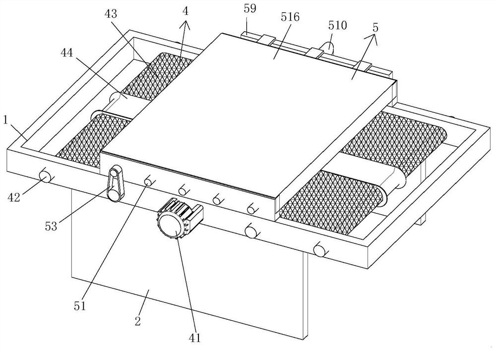
[0024] Such as Figure 1-4 As shown, the embodiment of the present invention provides a semiconductor processing equipment, including a support frame 1, a support base plate 2, a side plate 3, a transport mechanism 4 for transporting a semiconductor substrate, and a multilateral oven for drying a semiconductor substrate. Dry mechanism 5, the bottom of the support frame 1 is fixedly connected with the support base plate 2, the upper surface of the support frame 1 is fixedly con...


PUM


Abstract

The invention provides semiconductor machining equipment. The semiconductor machining equipment comprises a supporting frame, a supporting bottom plate, side plates, a transmission mechanism used for transmitting a semiconductor substrate and a multi-side drying mechanism used for drying the semiconductor substrate, wherein the bottom of the supporting frame is fixedly connected with the supporting bottom plate; and the two side plates which are symmetrically distributed with the center line of the supporting frame as a symmetric line are fixedly connected to the upper surface of the supporting frame. The invention relates to the field of semiconductor machining. According to the semiconductor machining equipment, the problems of low process coherence, incomplete drying and low efficiency in an existing semiconductor machining process are solved, and a special structure for realizing multi-surface and multi-roll-shaft synchronous work, dry flow and wet flow division transmission and multi-aspect drying is designed; and therefore, the problems that a semiconductor substrate cannot be simply adjusted by a common drying device, the semiconductor substrate needs more procedures to be distributed and collected during drying, and the semiconductor substrate is complex in integration and non-uniform in drying, so that the drying efficiency is influenced to a certain extent, are effectively solved.

Description

technical field [0001] The invention relates to the technical field of semiconductor processing, in particular to semiconductor processing equipment. Background technique [0002] With the development of society, semiconductors are used more and more widely. The conductivity of semiconductors is between metal conductors and insulators. Semiconductors need to be cleaned during processing. After cleaning, in order to quickly enter the process and continue processing, it is necessary to clean them. For drying treatment, the current drying of semiconductors is mainly carried out by ordinary drying boxes, but the size of semiconductor substrates is getting smaller and smaller, and a large number of semiconductor substrates are piled up. If the substrates are placed inside the drying box for drying To dry, careful arrangement is required to disperse the substrates as much as possible, otherwise it will easily lead to uneven drying, and when drying, the semiconductor substrates can...

Claims


Application Information

Patent Timeline
Patent Type & Authority Applications(China)
IPC IPC(8): F26B15/18F26B21/00F26B23/06F26B25/00F26B25/02H01L21/67H01L21/677
CPCF26B15/18F26B21/001F26B21/004F26B23/06F26B25/003F26B25/02H01L21/67034H01L21/6776
Inventor 汪剑敏
Owner 汪剑敏
Why Eureka
Try Eureka