
Void Detection Method for 3D NAND Memory

A technology for void detection and memory, which is used in semiconductor/solid-state device testing/measurement, semiconductor devices, electrical solid-state devices, etc., can solve problems such as leakage, affect the yield and production efficiency of 3DNAND memory products, and prevent abnormal leakage and improve The effect of production efficiency and product yield

Active Publication Date: 2022-05-17
YANGTZE MEMORY TECH CO LTD
View PDF3 Cites 0 Cited by
  • Summary
  • Abstract
  • Description
  • Claims
  • Application Information

AI Technical Summary

Problems solved by technology

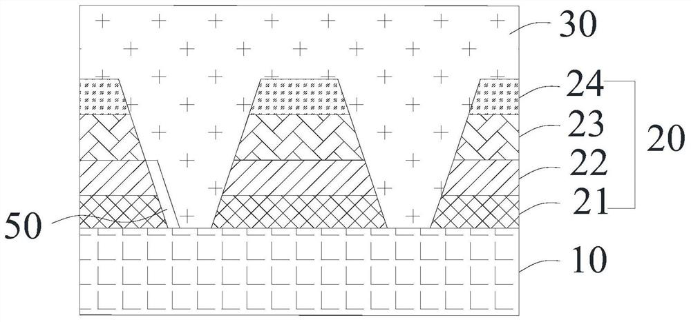
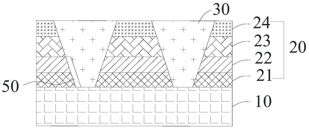
[0004] Wherein, during the process of forming the filling layer, a void may be formed in the filling layer, and after removing the sacrificial layer and filling the conductive material to form the gate, the void will make the bottom selective gate (BSG) communicate with the substrate, And cause abnormalities such as leakage, which in turn affects the product yield and production efficiency of 3D NAND memory

Method used


Image

  • Void Detection Method for 3D NAND Memory
  • Void Detection Method for 3D NAND Memory
  • Void Detection Method for 3D NAND Memory

Examples


Embodiment Construction

[0014] The following will clearly and completely describe the technical solutions in the embodiments of the application with reference to the drawings in the embodiments of the application. Apparently, the described embodiments are only some of the embodiments of the application, not all of them. Based on the embodiments in this application, all other embodiments obtained by persons of ordinary skill in the art without making creative efforts belong to the scope of protection of this application.

[0015] In the description of the present application, the terms "first", "second", etc. are used to distinguish different objects, not to describe a specific order or indicate the number of indicated technical features. In addition, the terms "upper", "inner ", "Outside", "Top", "Bottom", "Thickness" and other indicated orientations or positional relationships are based on the orientations or positional relationships shown in the drawings, and are only for the convenience of describi...


PUM

PropertyMeasurementUnit
thicknessaaaaaaaaaa
thicknessaaaaaaaaaa
thicknessaaaaaaaaaa

Abstract

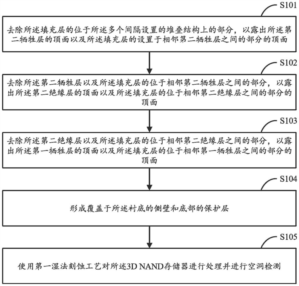
The present application provides a method for detecting holes in a 3D NAND memory, comprising: removing the part of the filling layer located on a plurality of stacked structures arranged at intervals; removing the second sacrificial layer and the part of the filling layer located adjacent to the second sacrificial layer The part between the layers; removing the second insulating layer and the part of the filling layer between the adjacent second insulating layers; forming a protective layer covering the sidewall and the bottom of the substrate; using the first wet method The etch process processes the 3D NAND memory and performs void detection. In the cavity detection method provided in the present application, the filling layer is partially removed to expose the top surface of the filling layer located between adjacent first sacrificial layers, and then the first wet etching process is used. The substrate is processed, and whether there is a hole in the filling layer is determined by detecting whether there is an etching trace on the substrate, so as to prevent abnormal leakage of the 3D NAND memory.

Description

technical field [0001] The present application relates to the technical field of memory manufacturing, in particular to a method for detecting voids in 3D NAND memory. Background technique [0002] NAND flash memory is a better storage device than hard disk drives, and it has been widely used in electronic products as people pursue non-volatile storage products with low power consumption, light weight and high performance. At present, the planar NAND flash memory is close to the limit of practical expansion. In order to further increase the storage capacity and reduce the storage cost per bit, a 3D NAND memory is proposed. [0003] At present, the manufacturing process of 3D NAND memory includes: forming a stack layer composed of insulating layers and sacrificial layers alternately stacked on the substrate; trimming and etching the stack layer to form a stack of multiple intervals in a stepped shape structure; forming a filling layer, and the filling layer fills the space a...

Claims


Application Information

Patent Timeline
Patent Type & Authority Patents(China)
IPC IPC(8): H01L21/66H01L27/11556H01L27/11582H10B41/27H10B43/27
CPCH01L22/12H10B41/27H10B43/27Y02D10/00
Inventor 韩烽陈金星马霏霏
Owner YANGTZE MEMORY TECH CO LTD
Learn More