Transfer bearing device and transfer method

A technology of a carrying device and a transfer method, which is applied in the manufacturing of electrical components, electric solid-state devices, semiconductor/solid-state devices, etc., can solve the problems of inability to achieve sufficient and accurate transfer, difficult chip spacing, and difficulty in repairing, and achieves a choice Sex transfer, improve transfer accuracy and transfer speed, and achieve the effect of selective repair

Inactive Publication Date: 2021-06-18
CHONGQING KONKA PHOTOELECTRIC TECH RES INST CO LTD
View PDF8 Cites 1 Cited by
  • Summary
  • Abstract
  • Description
  • Claims
  • Application Information

AI Technical Summary

Problems solved by technology

The crystal expansion process is time-consuming and labor-intensive, and it is difficult to ensure that the spacing of each chip is equal during the crystal expansion process, so that sufficient and accurate transfer cannot be achieved. For chips that fall off due to unsuccessful bonding, it is difficult to repair

Method used


Image

  • Transfer bearing device and transfer method
  • Transfer bearing device and transfer method
  • Transfer bearing device and transfer method

Examples


Embodiment Construction

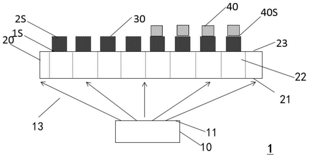
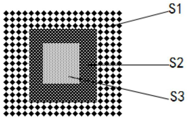
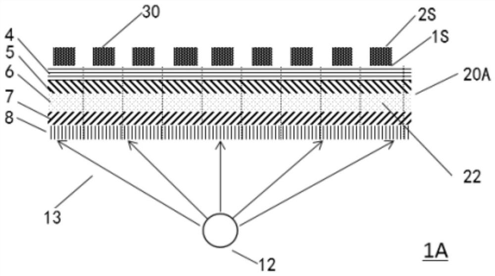
[0042] In order to facilitate the understanding of the present application, the present application will be described more fully below with reference to the relevant drawings. Preferred embodiments of the application are shown in the accompanying drawings. However, the present application can be embodied in many different forms and is not limited to the embodiments described herein. On the contrary, the purpose of providing these embodiments is to make the disclosure of the application more thorough and comprehensive.

[0043] Unless otherwise defined, all technical and scientific terms used herein have the same meaning as commonly understood by one of ordinary skill in the technical field to which this application belongs. The terminology used herein in the description of the application is only for the purpose of describing specific embodiments, and is not intended to limit the application.

[0044] As mentioned in the background technology section of the existing solution...


PUM


Abstract

The invention relates to a transfer bearing device and a transfer method. The transfer bearing device comprises a light source module, a light modulation module arranged on the light emitting side of the light source module and a plurality of transfer elements. The light modulation module comprises a light incident surface, a plurality of light control areas and a light emergent surface; the light incident surface is close to the light emergent side, the light emergent surface is far away from the light emitting side, and the light control areas are arranged between the light incident surface and the light emergent surface; each transfer element comprises a first surface and a second surface, the first surface is in contact with the light emergent surface of the light modulation module, and the second surface is used for placing a to-be-transferred micro element. The transfer method comprises the following steps: placing a to-be-transferred micro-component on a transfer component; enabling the target transfer positions on the target substrate to be aligned with the to-be-transferred micro-components one by one; turning on the light source module, enabling light emitted by the light source module to enter the light control area; and controlling the light entering the predetermined light control area to pass through the light emergent surface, and changing the shape of the corresponding transfer element to drive the micro-element on the transfer element to move. A wafer expansion process is not needed, selective transfer and repair can be realized, and the precision and the speed are high.

Description

technical field [0001] The invention relates to the technical field of micro-element transfer, in particular to a transfer carrier device and a transfer method. Background technique [0002] In the manufacturing process of Micro Light Emitting Diode (Micro-LED) display panels, because of the pursuit of more detailed display effects, the number of Micro-LED chips per unit area also increases geometrically, with millions or even tens of millions of chips. How to efficiently transfer Micro-LED chips from the growth substrate forming Micro-LED chips to the display backplane to complete the massive transfer is an urgent problem that needs to be solved. The existing mass transfer method is usually as follows: firstly, the growth substrate is bonded to the temporary storage substrate coated with photolytic glue or pyrolytic glue; then the growth substrate is peeled off by using lift-off technology; and then the temporary storage substrate is bonded to the display backplane. Carry ...

Claims


Application Information

Patent Timeline
Patent Type & Authority Applications(China)
IPC IPC(8): H01L21/683H01L33/48
CPCH01L21/6835H01L33/48H01L2221/68381
Inventor 李强许时渊
Owner CHONGQING KONKA PHOTOELECTRIC TECH RES INST CO LTD
Why Eureka
Try Eureka