


Quick Research
Generate reliable direction feasibility study reports for your R&D in just a few steps.

Technical Q&A
Discover and master advanced knowledge NOW. Basics, ideas, possibilities, all at once.

Find Solutions
As an expert in R&D theories, this can generate solutions to your technical problems instantly.

Evaluate Feasibility
Analyze your overall solution with one click, know your potential R&D risks in advance.

Monitor Landscape
Get weekly tech updates, stay abreast of the latest tech innovations and key insights.
A deep ultraviolet algan-based light-emitting diode with coupled quantum well structure
A technology for coupling quantum wells and light-emitting diodes, applied in semiconductor devices, electrical components, circuits, etc., can solve problems such as low luminous efficiency, achieve the effects of suppressing efficiency decline, reducing Auger recombination rate, and improving internal quantum efficiency
- Summary
- Abstract
- Description
- Claims
- Application Information
AI Technical Summary
Problems solved by technology
Method used
Image

Examples
Embodiment 1
[0017] This example discloses a coupling quantum well structure deep UV AlgaN-based air emitting diode, replacing the conventional well layer by the coupling well layer, adjusts the energy belt structure of the quantum well, expands the radiation composite region of the electron-hole in the well layer, thereby reducing The Russian compound rate increases the total spontaneous radiation composite rate, improves the internal quantum efficiency of the LED device, and suppresses the efficiency of the device.
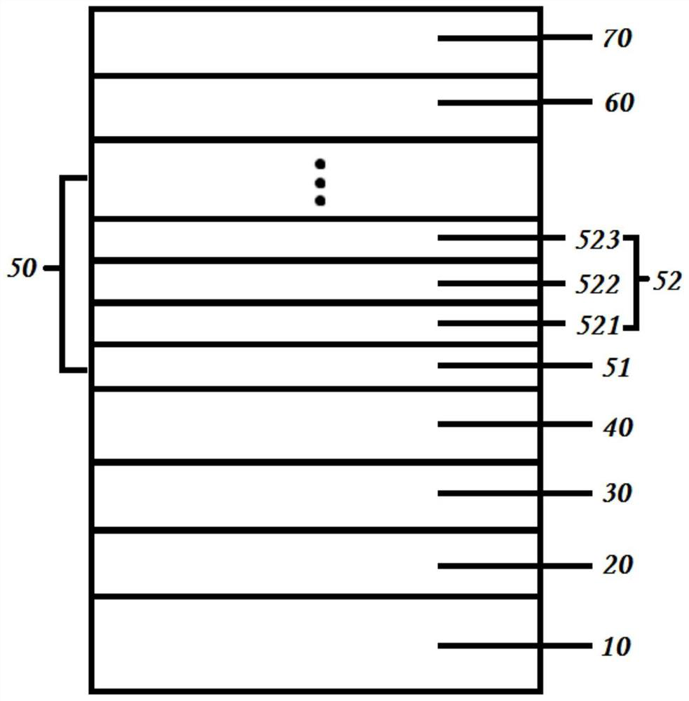
[0018] The embodiment of the present invention has an ultraviolet nitride light emitting diode of a coupling quantum well structure, such as figure 1 As shown, the substrate 10, the buffer layer 20, the superlattice layer 30, the N-type semiconductor layer 40, the multi-quantum well structure 50, the P-type semiconductor layer 60, and the p-type ohmic contact layer 70 are sequentially included. Among them, the multi-quantum well structure 50 is composed of a barrier layer 51 and...
Embodiment 2
[0029] This example discloses a coupling quantum well structure dark UV AlgaN-based air optical diode, the difference from Example 1 is that the well layer 52 consists of a 5-layer structure, from the bottom to the top to Al1 x GA 1-x N well layer 521, Al y GA 1-y N isolation layer 522, Al x GA 1-x N well layer 523 constitutes, Al y GA 1-y N isolation layer 524, Al x GA 1-x The N well layer 525 is composed, such as Figure 5 Indicated.
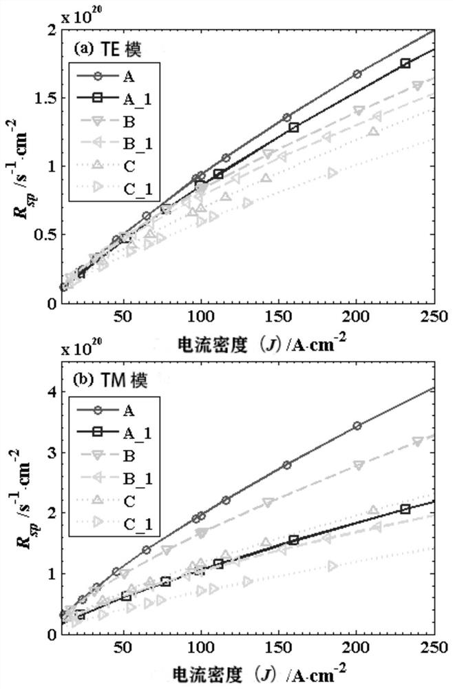
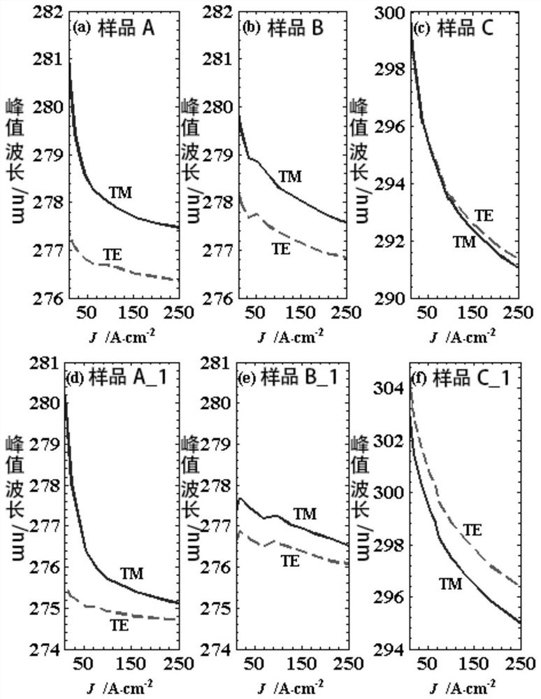
[0030] Image 6 The inner quantum efficiency of the coupling quantum well structure (sample XA) and the conventional quantum well structure (sample B and sample C) is provided for the potential well layer. The N-type semiconductor layer of sample XA is n-type Al 0.55 GA 0.45 N material; barrier is 8 nanometer thick Al 0.5 GA 0.5 N; Coupling well layer is 1 nanomerate Al 0.35 GA 0.65 N, 2 nanometer thick Al 0.5 GA 0.5 N, 1 nanometer thick al1 0.35 GA 0.65 N, 2 nanometer thick Al 0.5 GA 0.5 N, 1 nanometer thick al1 0.35 GA 0.65 N. From the figure, we...
PUM
| Property | Measurement | Unit |
|---|---|---|
| emission peak | aaaaa | aaaaa |
| thickness | aaaaa | aaaaa |
| thickness | aaaaa | aaaaa |
Abstract
Description
Claims
Application Information
 - R&D Engineer
- R&D Manager
- IP Professional
- Industry Leading Data Capabilities
- Powerful AI technology
- Patent DNA Extraction
Browse by: Latest US Patents, China's latest patents, Technical Efficacy Thesaurus, Application Domain, Technology Topic, Popular Technical Reports.
© 2024 PatSnap. All rights reserved.Legal|Privacy policy|Modern Slavery Act Transparency Statement|Sitemap|About US| Contact US: help@patsnap.com