Organic electroluminescent compound and organic electroluminescent device comprising the same

A compound and luminescent technology, applied in organic chemistry, luminescent materials, organic semiconductor devices, etc., can solve the problems of reduced device life, no specific disclosure of organic electroluminescent compounds, poor thermal stability, etc., and achieve the effect of improving the operating voltage

Pending Publication Date: 2021-06-08
ROHM & HAAS ELECTRONICS MATERIALS LLC
View PDF3 Cites 1 Cited by
  • Summary
  • Abstract
  • Description
  • Claims
  • Application Information

AI Technical Summary

Problems solved by technology

[0005] Although these materials provide good light-emitting characteristics, they have the following disadvantages: (1) Due to their low glass transition temperature and poor thermal stability, they may degrade during the high-temperature deposition process in vacuum and the lifetime of the device is reduced
Although organic electroluminescent devices containing phosphorescent host materials offer higher current efficiencies [cd / A] than organic electroluminescent devices containing fluorescent materials, they require considerably higher operating voltages
Therefore, there is no advantage in terms of power efficiency [lm / W]
(3) In addition, when these materials are used in organic electroluminescent devices, the operating life of organic electroluminescent devices is short and improvement in luminous efficiency is still required
However, the aforementioned references do not specifically disclose the organic electroluminescent compounds described in the present disclosure

Method used


Image

  • Organic electroluminescent compound and organic electroluminescent device comprising the same
  • Organic electroluminescent compound and organic electroluminescent device comprising the same
  • Organic electroluminescent compound and organic electroluminescent device comprising the same

Examples


example 1

[0111] Example 1: Preparation of Compound A-1

[0112]

[0113] 1) Synthesis of compound 2

[0114] In a reaction vessel, 7.3 g of compound 1 (18.2 mmol), 3.9 g of N-bromosuccinimide (NBS) (21.8 mmol), 180 mL of sulfuric acid, and 180 mL of acetic acid were added, and the mixture was stirred at room temperature for 18 hours. After the reaction was completed, water was added thereto for dilution. The resulting solid was obtained and then dried. The residue was purified by column chromatography to obtain 5.7 g of Compound 2 (yield: 66%).

[0115] 2) Synthesis of Compound 4

[0116] In a reaction vessel, 10 g of compound 3 (36.4 mmol), 11 g of bis(pinacolate) diboron (43.6 mmol), 0.32 g of bis(triphenylphosphine)palladium(II) dichloride (1.82 mmol), 10 g of potassium acetate (109.2 mmol), and 180 mL of 1,4-dioxane, and the mixture was stirred at 130° C. for 2 hours. After the reaction was completed, the reaction mixture was cooled to room temperature and the organic ...

example 2

[0130] Device Example 2: Production of OLEDs Comprising Compounds According to the Disclosure as Second Host

[0131] OLEDs were produced in the same manner as in Device Example 1, except that the light-emitting layer was formed as follows: the first host and the second host shown in Table 2 below were introduced as hosts into two chambers of a vacuum vapor deposition apparatus, respectively, and Compound D-50 was introduced as a dopant into another chamber. Evaporating the two host materials at different rates of 2:1, and simultaneously evaporating the dopant material at different rates, depositing the dopant at a doping amount of 10 wt% based on the total amount of host and dopant, A light emitting layer having a thickness of 40 nm was thus formed on the second hole transport layer.


PUM

PropertyMeasurementUnit
thicknessaaaaaaaaaa
thicknessaaaaaaaaaa
thicknessaaaaaaaaaa

Abstract

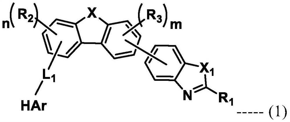
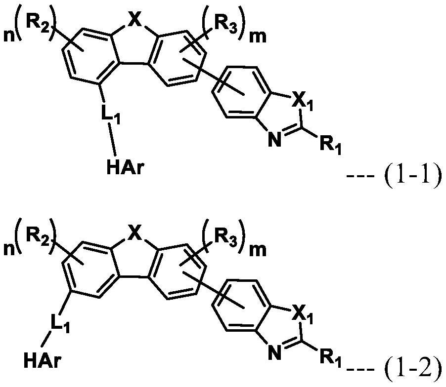
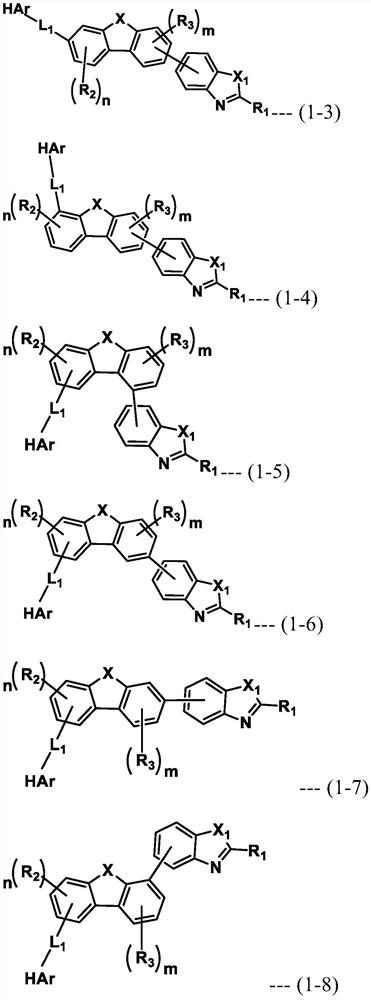
The present disclosure relates to an organic electroluminescent compound and an organic electroluminescent device comprising the same. By comprising the organic electroluminescent compound according to the present disclosure, it is possible to provide an organic electroluminescent device having improved driving voltage, luminous efficiency, lifetime and / or power efficiency properties.

Description

technical field [0001] The present disclosure relates to an organic electroluminescent compound and an organic electroluminescent device comprising the same. Background technique [0002] Electroluminescent (EL) devices are self-luminous display devices that have the advantage that they provide wider viewing angles, greater contrast ratios, and faster response times. The first organic electroluminescent device was developed by Eastman Kodak in 1987 by using small aromatic diamine molecules and aluminum complexes as materials for forming the light-emitting layer (see Appl. Phys . Lett. [Applied Physics Letters] 51, 913, 1987). [0003] The most important factor determining the luminous efficiency in an organic electroluminescent device is the luminescent material. Fluorescent materials have been widely used as light-emitting materials so far. However, in view of the mechanism of electroluminescence, phosphorescent light-emitting materials have been extensively studied sinc...

Claims


Application Information

Patent Timeline
Patent Type & Authority Applications(China)
IPC IPC(8): C07D413/14C07D417/14C09K11/06H01L51/50H01L51/54
CPCC07D413/14C07D417/14C09K11/06C09K2211/1011C09K2211/1029C09K2211/1033C09K2211/1037C09K2211/1059C09K2211/1088C09K2211/1092H10K85/615H10K85/654H10K85/657H10K85/6574H10K85/6576H10K50/12H10K85/342H10K50/11H10K2101/10H10K85/649C09K2211/1018
Inventor 金贤严智媛朴景秦李美子金侈植
Owner ROHM & HAAS ELECTRONICS MATERIALS LLC
Why Eureka
Try Eureka