


Quick Research
Generate reliable direction feasibility study reports for your R&D in just a few steps.

Technical Q&A
Discover and master advanced knowledge NOW. Basics, ideas, possibilities, all at once.

Find Solutions
As an expert in R&D theories, this can generate solutions to your technical problems instantly.

Evaluate Feasibility
Analyze your overall solution with one click, know your potential R&D risks in advance.

Monitor Landscape
Get weekly tech updates, stay abreast of the latest tech innovations and key insights.
Display panel, and preparation method thereof and display device
A display panel and display area technology, which is applied in semiconductor/solid-state device manufacturing, semiconductor devices, electrical components, etc., can solve the problems of packaging failure, shortened service life of organic light-emitting diode display devices, and inability to completely cover the organic layer film, etc., to achieve Improve packaging yield, avoid package failure, and improve service life
- Summary
- Abstract
- Description
- Claims
- Application Information
AI Technical Summary
Problems solved by technology
Method used
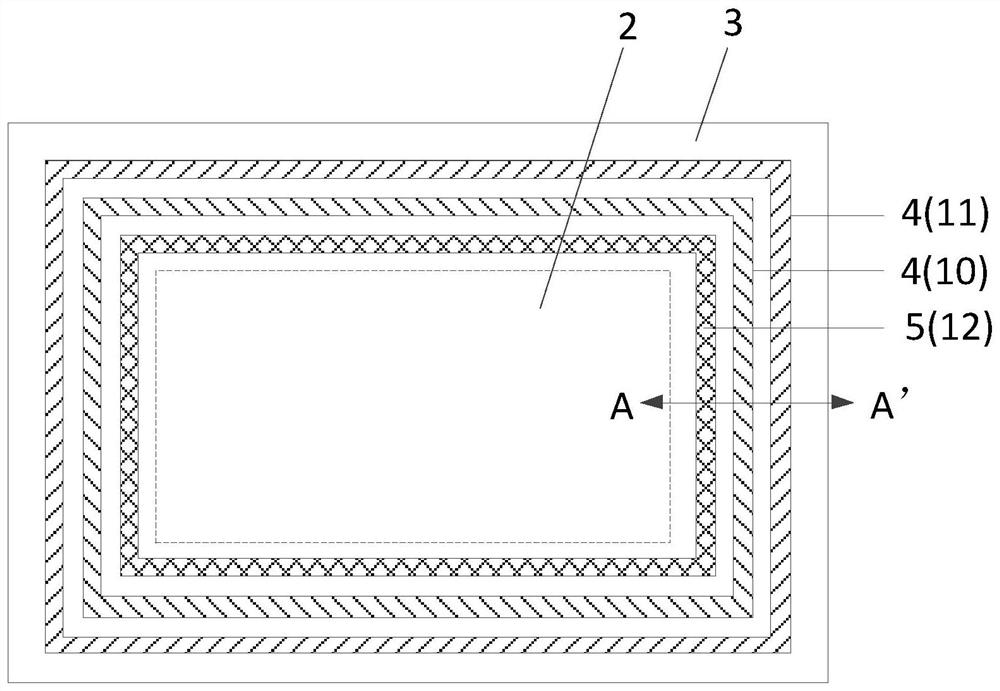
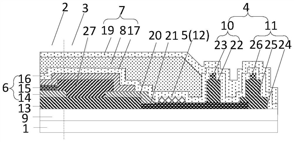
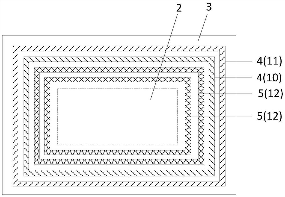
Image

Examples
Embodiment Construction
[0036] In order to make the purpose, technical solutions and advantages of the embodiments of the present application clearer, the technical solutions of the embodiments of the present application will be clearly and completely described below in conjunction with the drawings of the embodiments of the present application. Apparently, the described embodiments are some of the embodiments of the present application, but not all of them. And in the case of no conflict, the embodiments in the present application and the features in the embodiments can be combined with each other. Based on the described embodiments of the present application, all other embodiments obtained by persons of ordinary skill in the art without creative efforts shall fall within the protection scope of the present application.
[0037] Unless otherwise defined, the technical terms or scientific terms used in the application shall have the ordinary meanings understood by those skilled in the art to which th...
PUM
| Property | Measurement | Unit |
|---|---|---|
| thickness | aaaaa | aaaaa |
| particle diameter | aaaaa | aaaaa |
Abstract
Description
Claims
Application Information
 - R&D Engineer
- R&D Manager
- IP Professional
- Industry Leading Data Capabilities
- Powerful AI technology
- Patent DNA Extraction
Browse by: Latest US Patents, China's latest patents, Technical Efficacy Thesaurus, Application Domain, Technology Topic, Popular Technical Reports.
© 2024 PatSnap. All rights reserved.Legal|Privacy policy|Modern Slavery Act Transparency Statement|Sitemap|About US| Contact US: help@patsnap.com