Conductive assembly and testing device

A technology for conductive components and testing devices, which is applied in the directions of measuring devices, electronic circuit testing, measuring device casings, etc., can solve the problems of inconvenient assembly, high cost, and high processing cost, avoid electrical signal interference, improve service life, reduce The effect of production cost

Pending Publication Date: 2021-06-01
荀露
View PDF0 Cites 0 Cited by
  • Summary
  • Abstract
  • Description
  • Claims
  • Application Information

AI Technical Summary

Problems solved by technology

[0002] The development speed of semiconductors is getting faster and faster, and the integration level is getting higher and higher. With the development of 5G, the frequency of chips is getting higher and higher, and the requirements for chip testing technology are getting higher and higher. At present, traditional testing technology Spring probes are mainly used, and spring probes mainly have several shortcomings: one is that thin and short spring probes are difficult to manufacture and the cost is high; the other is that spring probes have spring components that have an inductive effect on electronic signals. There is interference, and high-frequency chips cannot be tested; the third is that the spring probe must be installed in the needle plate, and there are many micro-holes distributed on the needle plate. If such micro-holes are completed by machining, the processing cost will be very high , if it is finished by injection molding, the cost of the mold is high and the production cycle is long. Very thin, not easy to assemble, the cost of installing the probe is high, and the follow-up maintenance is also inconvenient. After the needle plate is damaged, the needle plate needs to be redone, and the maintenance cost is high

Method used


Image

  • Conductive assembly and testing device
  • Conductive assembly and testing device
  • Conductive assembly and testing device

Examples


Embodiment Construction

[0021] It should be understood that the specific embodiments described here are only used to explain the present invention, and are not intended to limit the present invention.

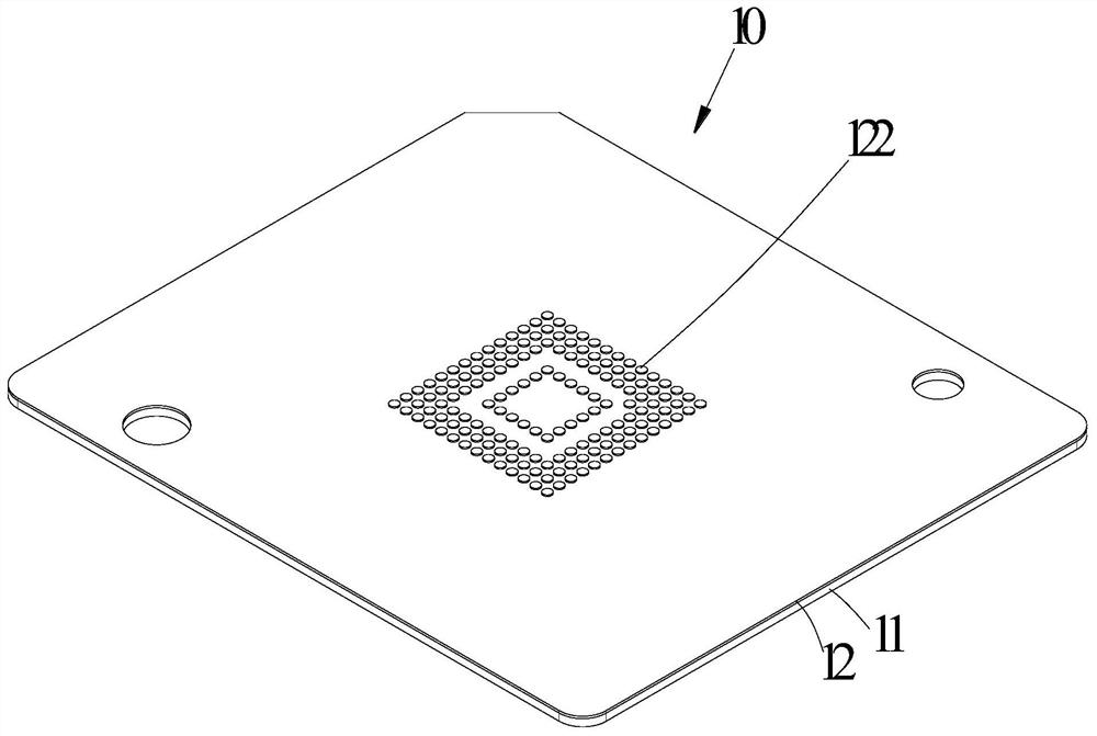
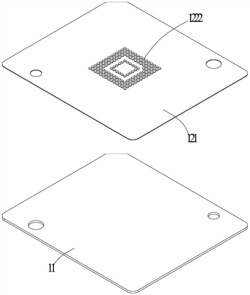
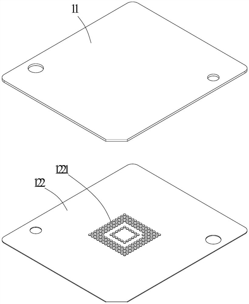
[0022] Such as Figure 1 to Figure 3 Shown is a preferred embodiment of the conductive assembly of the present invention, the conductive assembly is used in the testing device to electrically connect the circuit board for testing and the product under test, in this embodiment, the conductive assembly 10 includes elastic conductors 11 and protection plate 12, the elastic conductor 11 includes an elastic insulating plate body and a number of conductive particles distributed in the elastic insulating plate body. 11 When it is under pressure in the up and down direction, it conducts up and down in the pressure part; the protective plate 12 is arranged on the elastic conductor 11, and the protective plate 12 includes an insulating body 121 and is arranged on the insulating body 121. A plurality of conduct...


PUM


Abstract

The invention discloses a conductive assembly and a testing device. The conductive assembly comprises an elastic conductor and a protective plate, the elastic conductor comprises an elastic insulating plate body and a plurality of conductive particles distributed in the elastic insulating plate body, the elastic conductor is not conducted in the vertical direction and the left-right direction under the normal condition, and when the elastic conductor is pressed in the vertical direction, the elastic conductor is conducted above and below the pressed part; the protective plate is arranged on the elastic conductor and comprises an insulating body and a plurality of conductive columns arranged on the insulating body, the conductive columns penetrate through the insulating body, and the lower ends of the conductive columns protrude out of the lower surface of the insulating body to form first protruding columns; the first protruding columns are used for pressing the elastic conductor downwards during testing of the testing device so that the elastic conductor can be conducted up and down at the pressed position, and the circuit board for testing is electrically connected with the tested product. According to the invention, the manufacturing and maintenance cost can be reduced, and the conductive assembly and the testing device are suitable for testing chips with higher frequency.

Description

technical field [0001] The invention relates to the field of electronic testing devices, in particular to a conductive component and a testing device for testing integrated circuits and electronic devices. Background technique [0002] The development speed of semiconductors is getting faster and faster, and the integration level is getting higher and higher. With the development of 5G, the frequency of chips is getting higher and higher, and the requirements for chip testing technology are getting higher and higher. At present, traditional testing technology Spring probes are mainly used, and spring probes mainly have several shortcomings: one is that thin and short spring probes are difficult to manufacture and the cost is high; the other is that spring probes have spring components that have an inductive effect on electronic signals. There is interference, and high-frequency chips cannot be tested; the third is that the spring probe must be installed in the needle plate, ...

Claims


Application Information

Patent Timeline
Patent Type & Authority Applications(China)
IPC IPC(8): G01R31/28G01R1/04
CPCG01R1/0416G01R31/2884G01R31/2886
Inventor 荀露
Owner 荀露
Why Eureka
Try Eureka