Display panel and display device

A display panel and display area technology, applied to semiconductor devices, electrical components, circuits, etc., can solve problems such as differences, achieve the effects of improving consistency, improving display effects, and avoiding user experience

Active Publication Date: 2021-05-28
WUHAN CHINA STAR OPTOELECTRONICS SEMICON DISPLAY TECH CO LTD
View PDF6 Cites 7 Cited by
  • Summary
  • Abstract
  • Description
  • Claims
  • Application Information

AI Technical Summary

Problems solved by technology

Due to the high requirements of the optical performance of the camera area, the existing technology adopts the method of differentially designing the display panel area corresponding to the camera area to improve the light transmittance of the camera area, such as thinning or removing the light-shielding metal corresponding to the camera area, This will lead to a difference between the camera area and the normal display area of ​​the display panel. show the difference, need to come up with an effective solution

Method used


Image

  • Display panel and display device
  • Display panel and display device
  • Display panel and display device

Examples


Embodiment 1

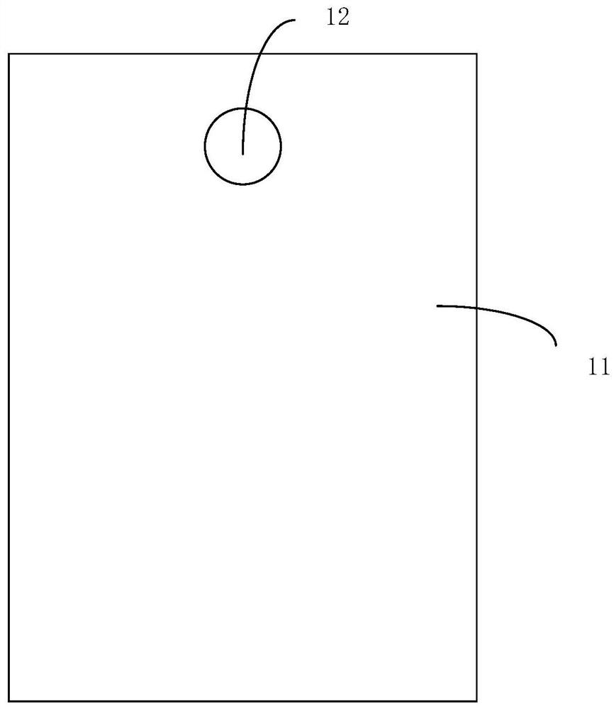
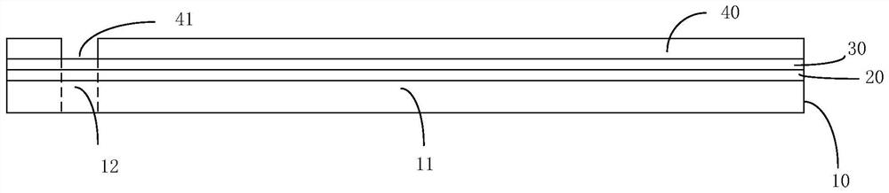
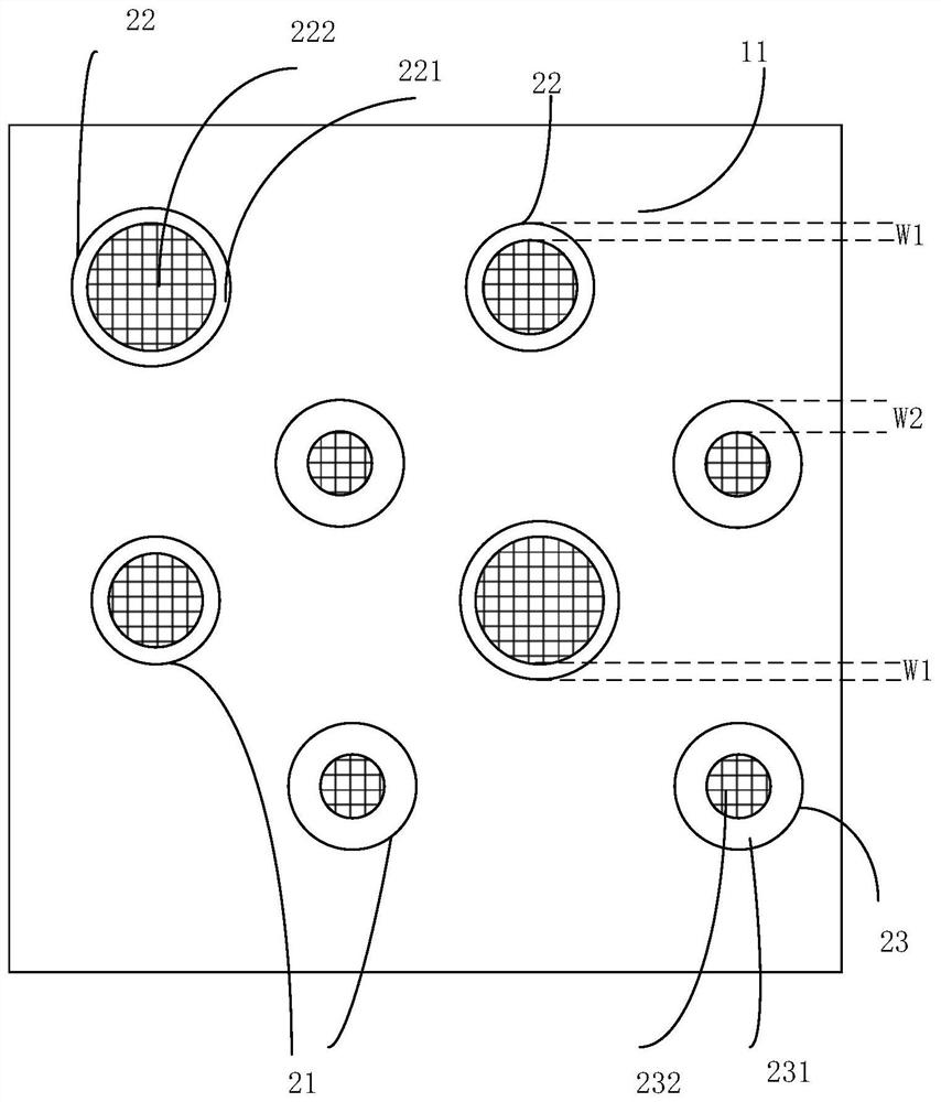
[0041] figure 1It is a top view of the display panel provided by Embodiment 1 of the present invention; figure 2 It is a front view of the display panel provided by Embodiment 1 of the present invention; image 3 It is a schematic structural diagram of the anode and the light emitting part of the pixel unit in the first display area provided by Embodiment 1 of the present invention. to combine Figure 1-Figure 3 As shown, Embodiment 1 of the present invention provides a display panel. The type of the display panel is, for example, an OLED display panel. The display panel includes: an array substrate 10 , a pixel layer 20 , an encapsulation layer 30 , and a touch control layer stacked in sequence. 40. The display panel is provided with a first display area 11 and a second display area 12, and the first display area 11 and the second display area 12 are arranged adjacent to each other. Specifically, a first display area 11 and a second display area 12 are respectively arrang...

Embodiment 2

[0064] Figure 7 It is a schematic structural diagram of the anode and the light emitting part of the pixel unit in the first display area provided by Embodiment 2 of the present invention. Such as Figure 7 As shown, the display panel and the display device disclosed in the second embodiment of the present invention are similar to the display panel and the display device in the first embodiment, and the same parts will not be repeated here in this embodiment. The difference is that the second width W2 of at least one second pixel unit 23 is greater than all the first widths W1 , and the second width W2 of other second pixel units is equal to the largest first width W1 . For example, in the first display area 11, the first width W1 of all the first pixel units 22 is the same; in every four second pixel units 23, the second width W2 of two second pixel units 23 is larger than the The first width W1, and the second width W2 of the other two second pixel units 23 are equal to t...

Embodiment 3

[0066] Figure 8 It is a schematic structural diagram of the anode and the light emitting part of the pixel unit in the first display area provided by Embodiment 3 of the present invention. Such as Figure 8 As shown, the display panel and the display device disclosed in the third embodiment of the present invention are similar to the display panel and the display device in the first embodiment, and the same parts will not be repeated here in this embodiment. The difference is that the pattern surrounded by the anode edge of the second pixel unit 22 is different from the pattern surrounded by the light emitting part edge of the second pixel unit 22 . In this embodiment, the anodes of all the second pixel units 23 in the first display area 11 of the display panel are rectangular, and the light emitting parts 232 of all the second pixel units 23 are circles, and the circle is located at the center of the rectangle. position, the width of the second part 231 of the anode of the...


PUM


Abstract

The invention discloses a display panel and a display device. The display panel comprises: an array substrate; a plurality of pixel units arranged on the array substrate, wherein each pixel unit comprises an anode, a light-emitting part and a cathode which are sequentially stacked; a packaging layer arranged on the plurality of pixel units; a touch control layer arranged on the packaging layer; and a first display area and a second display area, wherein the light transmittance of the touch control layer in the first display area is smaller than that of the touch control layer in the second display area, in the first display area, the multiple pixel units comprise first pixel units and second pixel units, and the minimum distance between the edge of the anode of at least one second pixel unit and the edge of the corresponding light-emitting part is larger than the minimum distance between the edge of the anode of the first pixel unit and the edge of the corresponding light-emitting part. According to the display panel and the display device, the display effect of the display panel under the large viewing angle is improved, and the problem that the user experience is reduced due to the brightness difference of the display panel under the large viewing angle is solved.

Description

technical field [0001] The present invention relates to display technology, in particular to a display panel and a display device. Background technique [0002] With the development of portable electronic devices (such as mobile phones, tablet computers, e-books and navigation equipment) industry, the technology of camera under panel (CUP) brings better visual enjoyment and uninterrupted all-round Display is gradually becoming a developing trend. [0003] The current CUP display device refers to a display device that can be displayed at the position of the camera. By increasing the light transmittance of the display panel in the display area corresponding to the camera (abbreviation: camera area), it can display the screen content normally when not taking pictures; When the light transmittance is good, it can meet the lighting requirements of the camera. Due to the high requirements of the optical performance of the camera area, the existing technology adopts the method of...

Claims


Application Information

Patent Timeline
IPC IPC(8): H01L27/32H01L51/52
CPCH10K59/351H10K59/353H10K59/40H10K50/813H10K59/352H10K59/122H10K59/121H10K59/65H10K59/80515
Inventor 刘威杨林孙业熙
Owner WUHAN CHINA STAR OPTOELECTRONICS SEMICON DISPLAY TECH CO LTD
Why Eureka
Try Eureka