Fast recovery diode and manufacturing method thereof
A technology for recovering diodes and anodes, which is applied in semiconductor/solid-state device manufacturing, electrical components, circuits, etc., and can solve problems such as high loss, long extraction time, and high device turn-off loss
- Summary
- Abstract
- Description
- Claims
- Application Information
AI Technical Summary
Problems solved by technology
Method used
Image

Examples
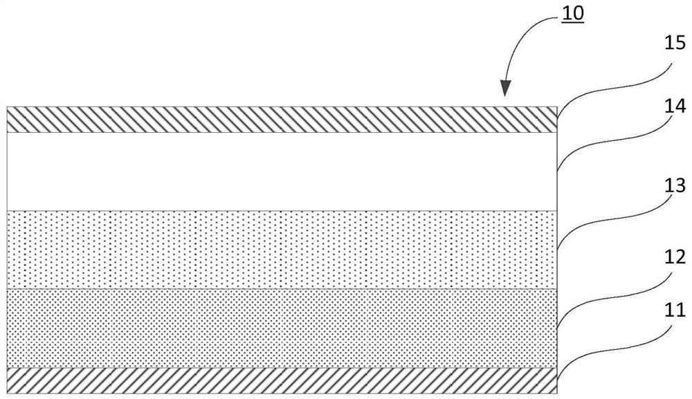
Embodiment 1
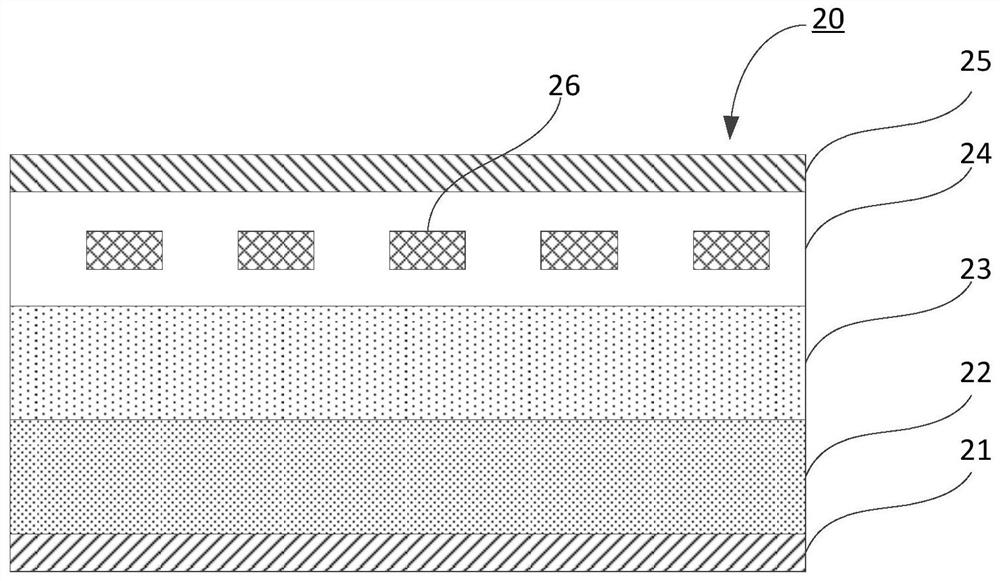
[0035] This embodiment provides a fast recovery diode 20 .
[0036] like Figure 2a As shown, the fast recovery diode 20 includes a substrate 23 , an anode region 24 , an N-type doped region 26 , an anode metal layer 25 , a cathode region 22 and a cathode metal layer 21 .
[0037] A substrate 23 made of a lightly doped N-type semiconductor, a cathode region 22 formed of a heavily doped N-type semiconductor is formed below the substrate 23, and an anode region 24 formed of a P-type semiconductor is formed above the substrate 23, Among them, in order to reduce the injection of holes, a low-doped P-type semiconductor is generally used as the anode region 24, and the N-type doped region 26 is embedded in the anode region 24; above the anode region 24 (the side away from the substrate 23) An anode metal layer 25 is formed, and a cathode metal layer 21 is formed under the cathode region 22 (a side away from the substrate 23 ).
[0038] The specific position of the N-type doped reg...
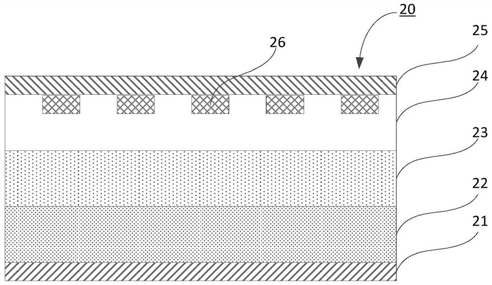
Embodiment 2
[0042] This embodiment provides a fast recovery diode 30 .
[0043] see Figure 3a The fast recovery diode 30 includes a substrate 33 , an anode region 34 , an N-type doped region 36 , an anode metal layer 35 , a buffer layer 37 , a cathode region 32 and a cathode metal layer 31 .
[0044] A substrate 33 made of a lightly doped N-type semiconductor, a cathode region 32 formed by a heavily doped N-type semiconductor is formed under the substrate 33, and a cathode region 32 formed by a heavily doped N-type semiconductor is formed with a lightly doped N-type semiconductor. An N-type semiconductor buffer layer 37 with a lower doping concentration than the cathode region 32 and a higher doping concentration than the substrate 33 is arranged between the substrates 33 made of N-type semiconductors, so that the N-type doping concentration gradient is formed to reduce the fast Recover the loss after the diode is turned on; an anode region 34 formed by a P-type semiconductor is formed ...
Embodiment 3
[0051] see Figure 4 , Figure 4 It is a schematic top view structure diagram of the fast recovery diode 40 shown in this embodiment. In this embodiment, the doped region 46 includes a plurality of annular sub-doped regions 46a to 46d arranged at intervals; further, a plurality of annular sub-doped regions arranged at intervals The sub-doped regions 46a to 46d are in the shape of concentric rings.
[0052] The cross-sectional structure of the fast recovery diode 40 is the same as that of the first or second embodiment, and will not be repeated here.
PUM
 Abstract
Description
Claims
Application Information
 - R&D
- Intellectual Property
- Life Sciences
- Materials
- Tech Scout
- Unparalleled Data Quality
- Higher Quality Content
- 60% Fewer Hallucinations
Browse by: Latest US Patents, China's latest patents, Technical Efficacy Thesaurus, Application Domain, Technology Topic, Popular Technical Reports.
© 2025 PatSnap. All rights reserved.Legal|Privacy policy|Modern Slavery Act Transparency Statement|Sitemap|About US| Contact US: help@patsnap.com