
A wavelength tunable semiconductor laser

A technology of lasers and semiconductors, which is applied in the direction of semiconductor lasers, lasers, laser components, etc., can solve the problems of not meeting the requirements of the light source, the modulation rate cannot be achieved, etc., to improve the direct modulation bandwidth, reduce the precision requirements, and improve the tolerance of process errors limited effect

Active Publication Date: 2022-02-11
HUAZHONG UNIV OF SCI & TECH
View PDF9 Cites 0 Cited by
  • Summary
  • Abstract
  • Description
  • Claims
  • Application Information

AI Technical Summary

Problems solved by technology

This scheme uses a tilted grating to effectively reduce the signal transmission damage caused by chirp during the direct modulation of the laser, improve the channel capacity, and realize the tuning function at the same time. It is also a high-quality relatively high-speed wavelength tunable light source, but its modulation rate Nor did it meet the 40GHz or higher requirements mentioned above
[0006] To sum up, most of the directly modulated lasers currently on the market or in the research field have only one function of high bandwidth or wavelength tunability, and a few lasers can obtain a modulation bandwidth below 20 GHz when realizing the wavelength tuning function, but they still cannot Meet the needs of the next generation of high-speed tunable light sources

Method used


Image

  • A wavelength tunable semiconductor laser
  • A wavelength tunable semiconductor laser
  • A wavelength tunable semiconductor laser

Examples


Embodiment Construction

[0030] In order to make the object, technical solution and advantages of the present invention clearer, the present invention will be further described in detail below in conjunction with the accompanying drawings and embodiments. It should be understood that the specific embodiments described here are only used to explain the present invention, not to limit the present invention.

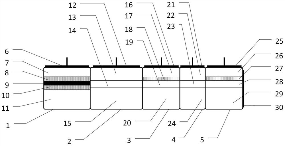
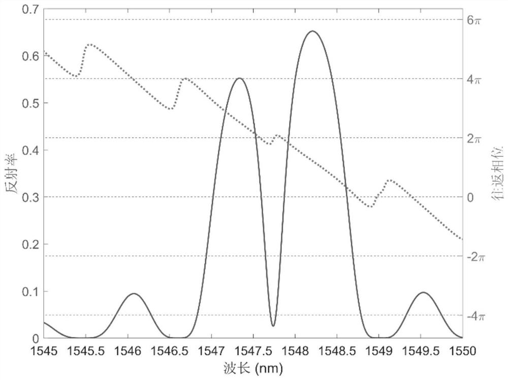
[0031] The purpose of the present invention is to provide a wavelength-tunable semiconductor laser, through the tuning of the current in the phase zone and the grating zone, the laser phase condition of the laser can be changed to achieve the tuning of the laser wavelength. At the same time, the sag introduced by the phase shift section is used to introduce a secondary mode to generate the PPR effect, which greatly improves the direct modulation bandwidth of the laser. The invention can not only tune the lasing wavelength in the range of about 7.5 nanometers, but also realize the highest direct mod...


PUM

PropertyMeasurementUnit
lengthaaaaaaaaaa
refractive indexaaaaaaaaaa

Abstract

The invention discloses a wavelength-tunable semiconductor laser, which includes an active region, a phase region, a grating region and a phase shift region fabricated in the grating region: the phase region consists of a second electrode, a second cladding layer and , the first waveguide layer and the second substrate; the first grating region is composed of the third electrode, the third cladding layer, the first grating layer, the second waveguide layer and the third substrate; the phase shift region Viewed from top to bottom, it is composed of the fourth electrode, the fourth cladding layer, the third waveguide layer and the fourth substrate; the structure of the second grating area is exactly the same as that of the first grating area. The left end face of the laser is the cleavage plane, from which the output light of the laser emerges. The right end face of the grating area is coated with an anti-reflection film to reduce the reflection of the end face inside the laser. The laser provided by the present invention realizes a high modulation bandwidth by introducing the photon-photon resonance effect, and can also realize a wavelength tuning function at the same time, so as to meet the requirements of the next-generation optical communication system for a high-performance, high-speed direct modulation wavelength tunable device.

Description

technical field [0001] The invention belongs to the technical field of optoelectronic devices, and more specifically relates to a distributed reflective semiconductor laser with adjustable wavelength and high-speed direct modulation. Background technique [0002] With the development of a series of information technologies such as smart applications, big data analysis, and cloud technology, our demand for data communication speed and capacity is increasing day by day. Institutions such as the Institute of Electrical and Electronics Engineers have also put forward requirements for light sources that can be applied to short-distance applications such as data centers. For example, in a 2-kilometer short-distance transmission link of 200GHz, it is necessary to use 4 modulation bandwidths of 40G to work in 4 Lasers of different wavelengths are used to form the light source. Therefore, in the access network, the highly demanded wavelength-tunable high-speed direct modulation semi...

Claims


Application Information

Patent Timeline
Patent Type & Authority Patents(China)
IPC IPC(8): H01S5/125H01S5/062
CPCH01S5/124H01S5/06233H01S5/06246
Inventor 刘也余永林
Owner HUAZHONG UNIV OF SCI & TECH
Learn More