
Micro LED device and transfer method thereof

A transfer method and technology of LED array, applied in the direction of electric solid device, semiconductor device, semiconductor/solid state device manufacturing, etc., can solve problems such as hindering LED pickup, reducing pickup efficiency, etc., to improve transfer efficiency, avoid poor electrical contact, Low pickup force requirement

Inactive Publication Date: 2021-03-09
NANJING CEC PANDA LCD TECH
View PDF0 Cites 1 Cited by
  • Summary
  • Abstract
  • Description
  • Claims
  • Application Information

AI Technical Summary

Problems solved by technology

[0003] When separating the LED from the growth substrate, glue such as UV glue or pyrolytic glue is generally used as a temporary fixing material, and the glue can provide a buffer for the stress generated during the separation of the LED and prevent the LED from breaking, but the glue will remain on the surface of the LED and affect the electrical current. Sexual contact, and there is still some sticky force after the glue is debonded, which hinders the LED pickup and reduces the pickup efficiency

Method used


Image

  • Micro LED device and transfer method thereof
  • Micro LED device and transfer method thereof
  • Micro LED device and transfer method thereof

Examples


Embodiment Construction

[0032] Below in conjunction with accompanying drawing and specific embodiment, further illustrate the present invention, should be understood that these embodiments are only for illustrating the present invention and are not intended to limit the scope of the present invention, after having read the present invention, those skilled in the art will understand various aspects of the present invention Modifications in equivalent forms all fall within the scope defined by the appended claims of this application.

[0033] In order to make the drawing concise, each drawing only schematically shows the parts related to the present invention, and they do not represent the actual structure of the product. In addition, to make the drawings concise and easy to understand, in some drawings, only one of the components having the same structure or function is schematically shown, or only one of them is marked. Herein, "a" not only means "only one", but also means "more than one".

[0034] ...


PUM


Abstract

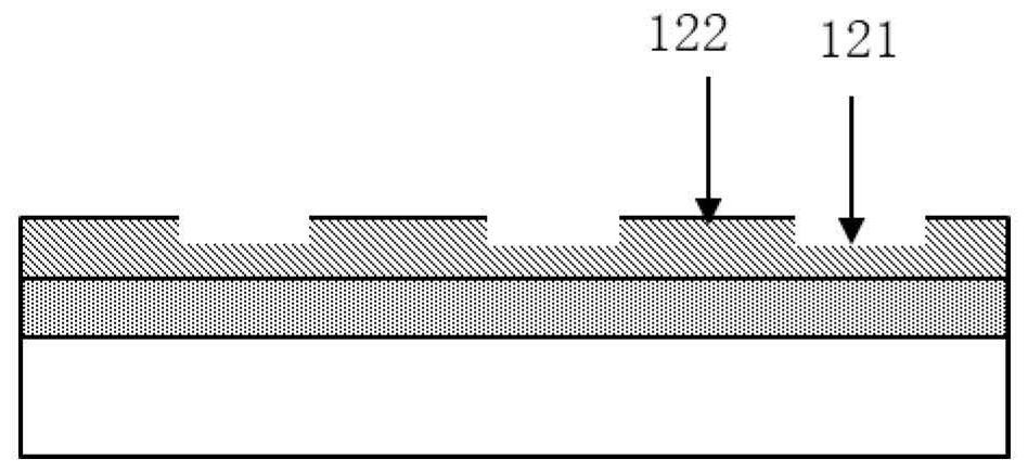
The invention further provides a Micro LED device and a transfer method thereof. The Micro LED device comprises a glass substrate, a glue buffer layer located on the glass substrate, a second metal protrusion located on the glue buffer layer, an adhesive layer and an LED array, wherein the second metal protrusion is in a concave-convex shape, the adhesive layer is located on the convex shape of the second metal protrusion, and the LED array comprises a first metal protrusion located in the concave shape of the second metal protrusion and an epitaxial layer located on the first metal protrusion. The LED metal layer of the LED array is placed in the concave part of the second metal protrusion and is not in direct contact with the glue buffer layer, so that no glue is left when the LED arrayis transferred; on the other hand, no glue is arranged at the bottom of the LED array, so that when the LED array is transferred, the requirement for picking force is small, the transfer efficiency isimproved, and poor electrical contact of LEDs is avoided.

Description

technical field [0001] The present invention relates to the technical field of Micro LED, in particular to a Micro LED display device and a transfer method thereof. Background technique [0002] Micro LED is an inorganic light-emitting material that has the advantages of high luminous efficiency, long life, and high reliability, and has been widely concerned. In order to make a full-color display, it is necessary to process three colors of micro LEDs of R, G, and B from their respective growth substrates. Pick up and place on the drive backplane to separate the LED from the growth substrate. Generally, a laser lift-off device is used to temporarily fix the LED on the transient substrate and wait for transfer. [0003] When separating the LED from the growth substrate, glue such as UV glue or pyrolytic glue is generally used as a temporary fixing material, and the glue can provide a buffer for the stress generated during the separation of the LED and prevent the LED from brea...

Claims


Application Information

Patent Timeline
Patent Type & Authority Applications(China)
IPC IPC(8): H01L21/78H01L21/683H01L27/15
CPCH01L21/6835H01L21/7806H01L27/156H01L2221/68368
Inventor 张有为周宇朱充沛高威
Owner NANJING CEC PANDA LCD TECH
Learn More