Carrier plate for LED wafer manufacturing process

A technology of wafers and trays, which is applied in the field of trays in the LED wafer manufacturing process, can solve the problems of insufficient wafer evaporation and low productivity of trays, and achieve the goal of improving the utilization rate of trays, increasing production capacity, and increasing the number of trays. Effect

Pending Publication Date: 2020-11-13
XIAMEN QIANZHAO SEMICON TECH CO LTD
View PDF0 Cites 1 Cited by
  • Summary
  • Abstract
  • Description
  • Claims
  • Application Information

AI Technical Summary

Problems solved by technology

[0005] In view of this, the present invention provides a carrier for LED wafer manufacturing process, which solves the problem of low productivity of the carrier and wafer evaporation in the background technology without increasing the size of the carrier or modifying other hardware of the PVD machine. Insufficient plating problem

Method used


Image

  • Carrier plate for LED wafer manufacturing process
  • Carrier plate for LED wafer manufacturing process
  • Carrier plate for LED wafer manufacturing process

Examples


Embodiment Construction

[0045] In order to make the content of the present invention clearer, the content of the present invention will be further described below in conjunction with the accompanying drawings. The invention is not limited to this specific example. Based on the embodiments of the present invention, all other embodiments obtained by persons of ordinary skill in the art without making creative efforts belong to the protection scope of the present invention.

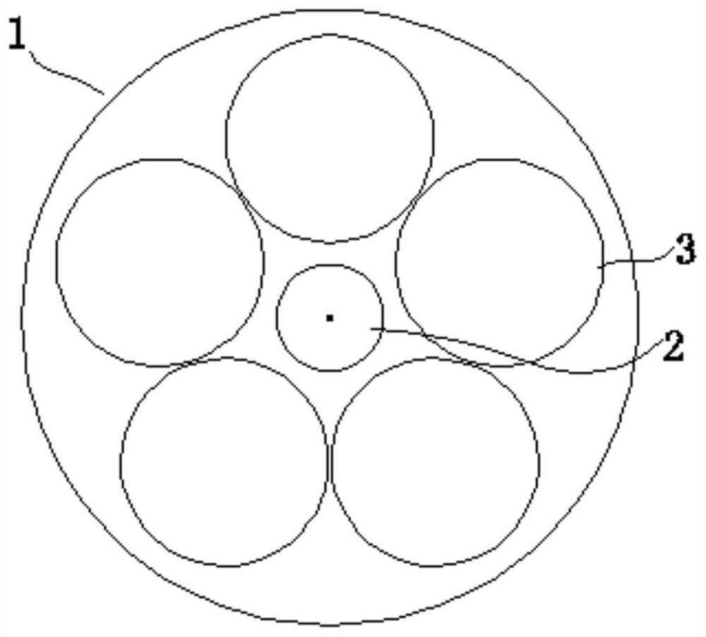
[0046] A carrier plate used in the LED wafer manufacturing process provided by this embodiment, such as Figure 4 shown, including:

[0047] A carrier plate 1;

[0048] A wafer placement surface is provided on the tray 1, and the wafer placement surface is circular;

[0049] Wafer placement slots are provided on the wafer placement surface, and the wafer placement slots include a central wafer placement slot 2 and a number of peripheral wafer placement slots 3; each peripheral wafer placement slot 3 is set around the center wafe...


PUM

PropertyMeasurementUnit
widthaaaaaaaaaa
lengthaaaaaaaaaa
lengthaaaaaaaaaa

Abstract

The invention provides a carrier plate for an LED wafer manufacturing process. The carrier plate comprises a carrier plate body; the carrier plate body is provided with a wafer placing surface, the wafer placing surface is provided with a wafer placing groove, and the wafer placing groove comprises a central wafer placing groove and a plurality of peripheral wafer placing grooves; the peripheral wafer placing grooves are arranged around the center of the central wafer placing groove; and each peripheral wafer placing groove is provided with a baffle, and each baffle is positioned at the flat edges of the corresponding peripheral wafer placing groove and the carrier plate body. Each peripheral wafer placing groove connected with the edge of the carrier plate body is arranged, so that the number of the wafer placing grooves is increased, and the productivity is improved; and meanwhile, every two adjacent peripheral wafer placing grooves are close to each other and form a clearance inclined plane with the edge of the carrier plate body, and the inclined planes can improve the temperature field and the flow field of the edge area of the carrier plate, improve the efficiency of depositing mixed gas and solve the problem of poor uniformity of peripheral wafers.

Description

technical field [0001] The invention belongs to the technical field of semiconductors, and more specifically relates to a carrier plate used for LED wafer manufacturing process. Background technique [0002] III-V nitrides, due to their direct bandgap semiconductor characteristics, have excellent physical properties such as large forbidden band width, high breakdown electric field, and high electron saturation mobility, and have received extensive attention in the fields of electronics and optics. Among them, GaN-based light-emitting diodes have made great progress in lighting, display, and digital. Studies have shown that using PVD (Physical Vapor Deposition, physical vapor deposition) to evaporate a layer of AlN buffer layer on the sapphire substrate, and then epitaxial GaN material can significantly improve the quality of GaN-based LED crystals, thereby significantly improving the performance of LED devices. This processing technology of patterned sapphire substrate comb...

Claims


Application Information

Patent Timeline
Patent Type & Authority Applications(China)
IPC IPC(8): C23C14/50C23C14/24C23C14/06C23C14/34
CPCC23C14/50C23C14/24C23C14/34C23C14/0617
Inventor 林志园洪金居陈火宾肖遥程伟
Owner XIAMEN QIANZHAO SEMICON TECH CO LTD
Why Eureka
Try Eureka