
PCB structure for wiring of electrostatic protection device and signal test equipment

A technology of electrostatic protection devices and PCB boards, which is applied in the direction of electrical components, printed circuit components, circuit devices, etc., and can solve problems such as sudden changes in impedance

Inactive Publication Date: 2020-10-23
WUHAN JINGCE ELECTRONICS GRP CO LTD +1
View PDF5 Cites 0 Cited by
  • Summary
  • Abstract
  • Description
  • Claims
  • Application Information

AI Technical Summary

Problems solved by technology

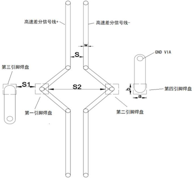
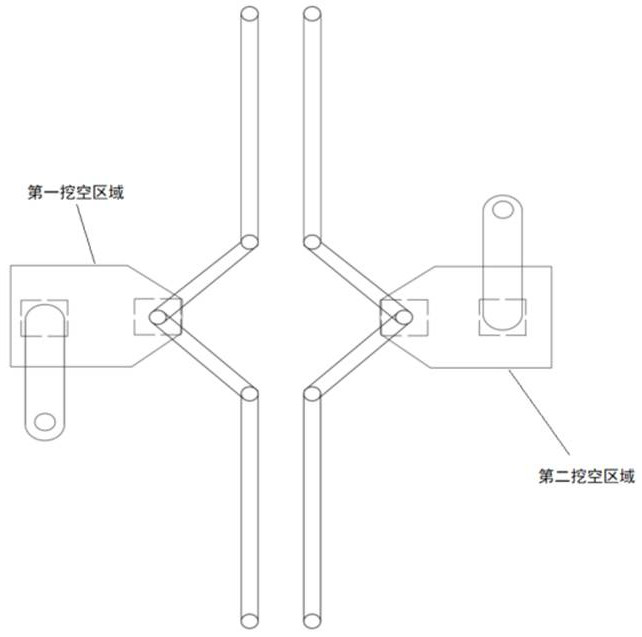
[0004] In view of the above defects or improvement needs of the prior art, the present invention provides a PCB board structure and signal testing equipment for the wiring of electrostatic protection devices, which mainly solves the problem of improving the inconsistency between the pads and transmission lines of electrostatic protection devices through PCB layout. Signal quality issues caused by abrupt impedance changes

Method used


Image

  • PCB structure for wiring of electrostatic protection device and signal test equipment
  • PCB structure for wiring of electrostatic protection device and signal test equipment

Examples


Embodiment Construction

[0025] In order to make the object, technical solution and advantages of the present invention clearer, the present invention will be further described in detail below in conjunction with the accompanying drawings and embodiments. It should be understood that the specific embodiments described here are only used to explain the present invention, not to limit the present invention.

[0026] In addition, the technical features involved in the various embodiments of the present invention described below can be combined with each other as long as they do not constitute a conflict with each other. The present invention will be further described in detail below in combination with specific embodiments.

[0027] The technical terms involved in the present invention are explained as follows:

[0028] ESD (Electrostatic Discharge Protection Devices), also known as transient voltage suppression diode array (TVS Array), is a single or multi-channel ESD with specific functions designed b...


PUM


Abstract

The invention discloses a PCB structure for wiring of an electrostatic protection device and signal test equipment. The GND layers are arranged in multiple layers, and corresponding hollowing processing is carried out on the orthographic projection area of the electrostatic protection device in the first GND layer, so that a first hollow area and a second hollow area contain orthographic projection areas of the signal lines on the first GND layer as few as possible, and high impedance of the transmission line caused by hollowing out the reference layer under the transmission lines can be avoided; and meanwhile, the place right under a bonding pad where the signal of the electrostatic protection device passes is hollowed out, so that the impedance formed after hollowing needs to meet the characteristic impedance requirement of the signal line, and the impedance of the signal, particularly a high-speed signal, passing through the PCB transmission line can be more continuous.

Description

technical field [0001] The invention belongs to the field of PCB board design, and in particular relates to a PCB board structure and signal testing equipment for wiring of electrostatic protection devices. Background technique [0002] In a circuit with resistance, inductance and capacitance, the obstruction to the signal in the circuit is called impedance, and the common impedance term for PCB is "characteristic impedance". When the electronic equipment is in operation, the signal sent by the driving element will be transmitted to the receiving element through the transmission line on the PCB. When the signal is transmitted in the transmission line on the PCB, its characteristic impedance must match the impedance of the driving element and the receiving element. In this way, The energy can be completely transmitted. Once the transmission line impedance on the PCB changes suddenly, the transmitted signal will have problems such as reflection, loss, attenuation, etc., which ...

Claims


Application Information

Patent Timeline
IPC IPC(8): H05K1/02
CPCH05K1/0245H05K1/025H05K1/0251
Inventor 易小鹭
Owner WUHAN JINGCE ELECTRONICS GRP CO LTD
Learn More