Manufacturing method of semiconductor device

A manufacturing method and semiconductor technology, applied in the direction of semiconductor devices, electrical solid devices, electrical components, etc., can solve the problems of split-gate flash memory failure, short floating gate width, etc.

Inactive Publication Date: 2020-10-20
SHANGHAI HUAHONG GRACE SEMICON MFG CORP
View PDF5 Cites 0 Cited by
  • Summary
  • Abstract
  • Description
  • Claims
  • Application Information

AI Technical Summary

Problems solved by technology

[0008] The object of the present invention is to provide a manufacturing method of a semiconductor device to solve the problem that the floating gate width is relatively short due to the thin sidewall thickness in the split-gate flash memory, which makes the split-gate flash memory prone to failure during programming.

Method used


Image

  • Manufacturing method of semiconductor device
  • Manufacturing method of semiconductor device
  • Manufacturing method of semiconductor device

Examples


Embodiment Construction

[0039] The manufacturing method of the semiconductor device proposed by the present invention will be further described in detail below with reference to the accompanying drawings and specific embodiments. It should be noted that all the drawings are in a very simplified form and use imprecise scales, and are only used to facilitate and clearly assist the purpose of illustrating the embodiments of the present invention. In addition, the structures shown in the drawings are often a part of the actual structure. In particular, each drawing needs to display different emphases, and sometimes uses different scales.

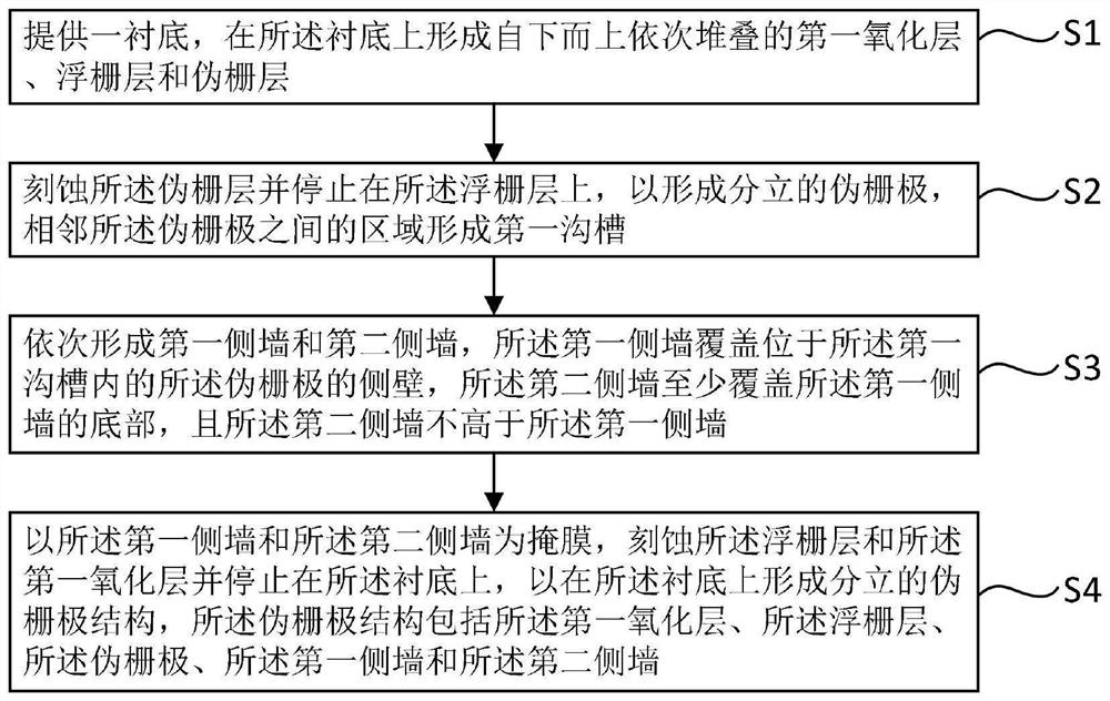
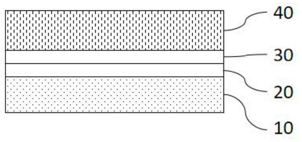
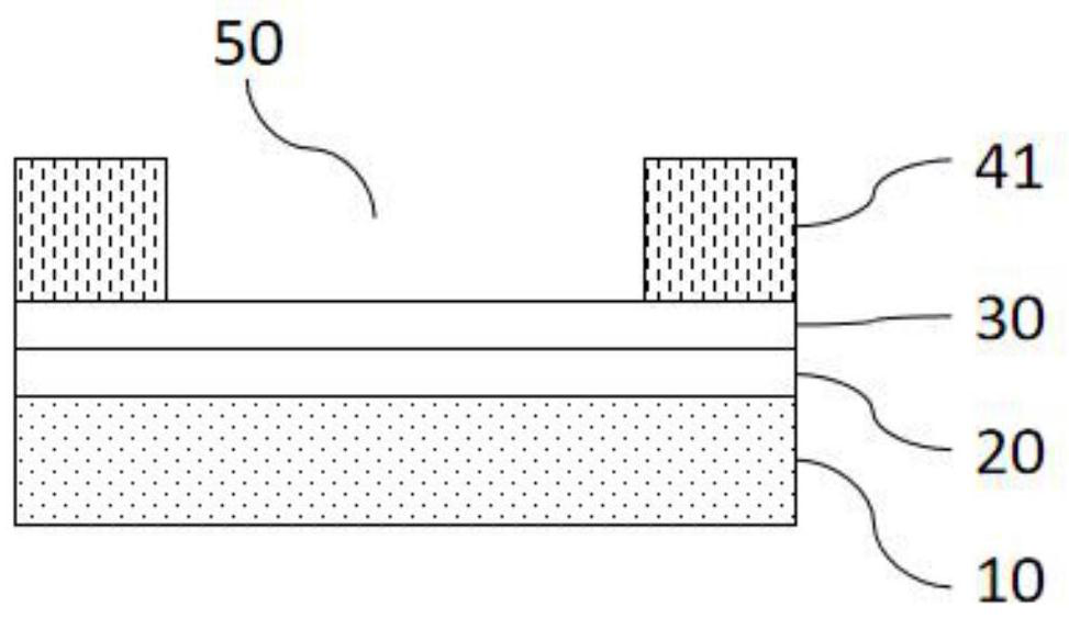
[0040] This embodiment provides a method for manufacturing a semiconductor device, such as figure 1 shown, including:

[0041] S1, providing a substrate on which a first oxide layer, a floating gate layer and a dummy gate layer are sequentially stacked from bottom to top;

[0042] S2, etching the dummy gate layer and stopping on the floating gate layer to form discr...


PUM

PropertyMeasurementUnit
thicknessaaaaaaaaaa

Abstract

The invention provides a manufacturing method of a semiconductor device. The manufacturing method comprises the steps: forming a first oxide layer, a floating gate layer and a pseudo gate layer whichare stacked in sequence from bottom to top on a substrate; etching the pseudo gate layer to form a pseudo gate; forming a first side wall and a second side wall sequentially, covering the side wall ofa pseudo gate by the first side wall, at least covering the bottom of the first side wall by the second side wall, and enabling the second side wall not to be higher than the first side wall; and etching the floating gate layer and the first oxide layer by taking the first side wall and the second side wall as masks and stopping on the substrate. The first side wall is formed; the second side wall is formed at the bottom of the first side wall, the thickness of the side wall is increased; the floating gate layer is etched by taking the first side wall and the second side wall as masks; due tothe fact that the thickness of the side wall is increased and the long floating gate layer is reserved, the turn-off capacity of a channel is enhanced, and the problem that the split-gate flash memory is prone to fail in the programming process due to the fact that the length of a floating gate of the split-gate flash memory is shortened because the thickness of the side wall is small is solved.

Description

technical field [0001] The invention relates to the technical field of semiconductors, in particular to a method for manufacturing a semiconductor device. Background technique [0002] Random access memory (such as DRAM and SRAM) has the problem of data loss after power failure during use. [0003] In order to overcome this problem, various flash memories have been designed and developed. The flash memory based on the floating gate concept has become a more general flash memory due to its smaller cell size and good working performance. [0004] Flash memory includes two basic structures: gate stack (stackgate) and split gate (splitgate) structure. Among them, the gate stack flash memory includes: a tunnel oxide layer formed on the semiconductor substrate in sequence, a floating silicon nitride layer for storing electrons, a control oxide layer, and a control gate polysilicon layer for controlling electron storage and release. , that is, the SONOS structure. [0005] The ...

Claims


Application Information

Patent Timeline
Patent Type & Authority Applications(China)
IPC IPC(8): H01L21/28H01L27/11521H01L29/423H10B41/30
CPCH01L29/401H01L29/42324H01L29/42356H10B41/30
Inventor 汤志林王卉付永琴孙琪
Owner SHANGHAI HUAHONG GRACE SEMICON MFG CORP
Why Eureka
Try Eureka