Substrate processing device and substrate processing method
A substrate processing device and a technology for a substrate processing method are applied in the directions of measuring devices, cleaning methods and utensils, chemical instruments and methods, etc., and can solve the problems of uneven processing quality of multiple substrates.
- Summary
- Abstract
- Description
- Claims
- Application Information
AI Technical Summary
Problems solved by technology
Method used
Image
Examples
no. 1 approach >
[0048]
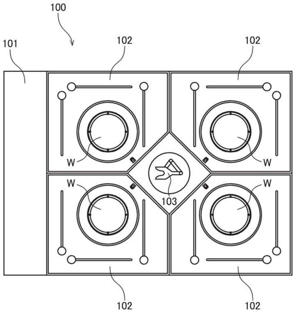
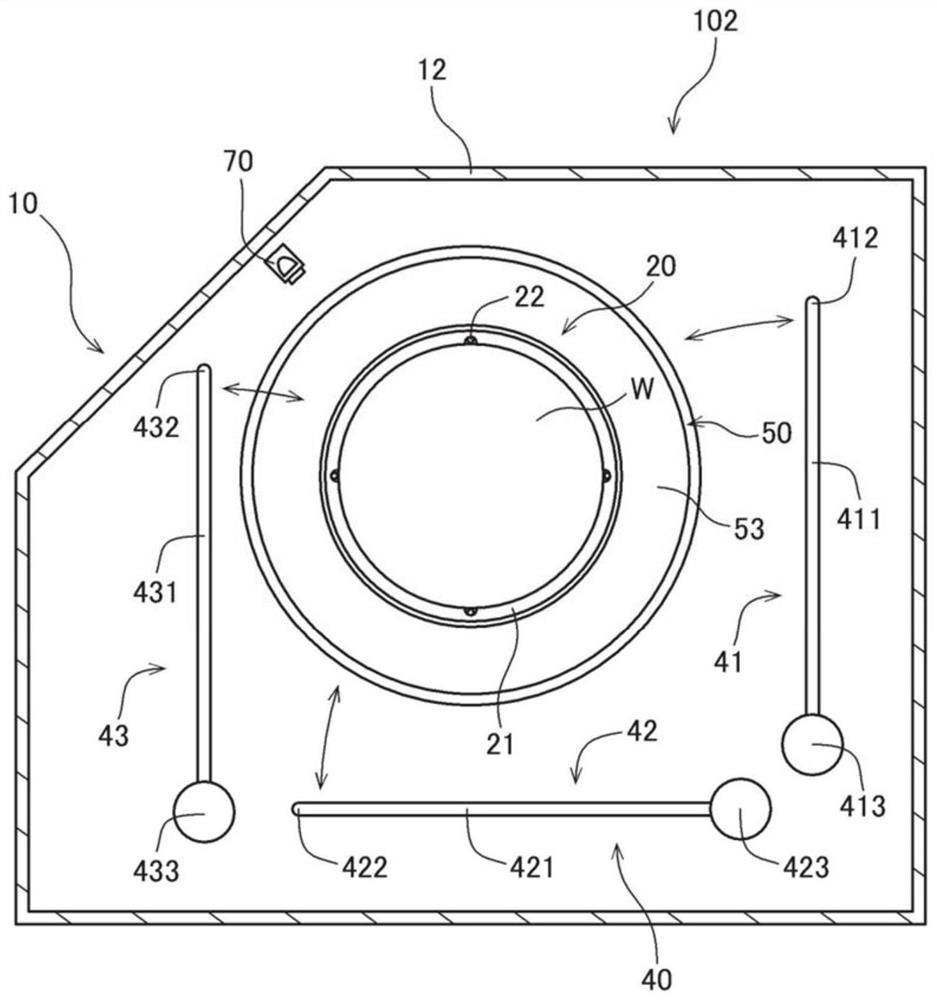
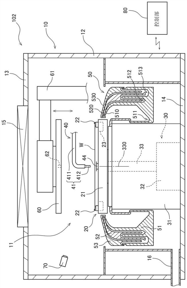
[0049] figure 1 It is a plan view of the substrate processing apparatus 100 according to the first embodiment of the present invention. The substrate processing apparatus 100 is an apparatus for supplying a processing liquid to the surface of a disk-shaped substrate W (silicon substrate) to process the surface of the substrate W in a semiconductor wafer manufacturing process. Such as figure 1As shown, the substrate processing apparatus 100 includes an indexer (indexer) 101 , a plurality of processing units 102 and a main transfer robot (robot) 103 .
[0050] The indexer 101 is used to carry in the unprocessed substrate W from the outside and carry out the processed substrate W to the outside. In the indexer 101, a plurality of carriers (carriers) accommodating a plurality of substrates W are arranged. In addition, the indexer 101 includes a transfer robot not shown. The transfer robot transfers the substrate W between the carrier in the indexer 101 and the proce...
no. 2 approach >
[0108] Next, a second embodiment of the present invention will be described. In the second embodiment, the structure itself of the substrate processing apparatus 100 is the same as that of the first embodiment, and the processing procedure is also the same except for a part. Hereinafter, overlapping descriptions of the same contents as those in the first embodiment will be omitted.
[0109] Figure 8 It is a flowchart showing the flow of the first processing and the second processing in the second embodiment.
[0110] In the second embodiment, steps S1 to S6 are performed in the same manner as in the first embodiment. That is, first, the model substrate Wd is carried into the chamber 10 (step S1). Next, the first process is performed on the model substrate Wd in the chamber 10 (step S2 to step S4). When the first process ends, the thermal imaging camera 70 measures the temperature of the target area A (step S5). Next, the control unit 80 determines whether or not the seco...
PUM
 Abstract
Description
Claims
Application Information
 - R&D
- Intellectual Property
- Life Sciences
- Materials
- Tech Scout
- Unparalleled Data Quality
- Higher Quality Content
- 60% Fewer Hallucinations
Browse by: Latest US Patents, China's latest patents, Technical Efficacy Thesaurus, Application Domain, Technology Topic, Popular Technical Reports.
© 2025 PatSnap. All rights reserved.Legal|Privacy policy|Modern Slavery Act Transparency Statement|Sitemap|About US| Contact US: help@patsnap.com


