


Quick Research
Generate reliable direction feasibility study reports for your R&D in just a few steps.

Technical Q&A
Discover and master advanced knowledge NOW. Basics, ideas, possibilities, all at once.

Find Solutions
As an expert in R&D theories, this can generate solutions to your technical problems instantly.

Evaluate Feasibility
Analyze your overall solution with one click, know your potential R&D risks in advance.

Monitor Landscape
Get weekly tech updates, stay abreast of the latest tech innovations and key insights.
High-performance wafer-level lead sulfide near-infrared photosensitive film and preparation method thereof
A near-infrared light and thin film preparation technology, which is applied in vacuum evaporation plating, coating, electric solid devices, etc., can solve the problems of lack of reproducibility and low sensitivity
- Summary
- Abstract
- Description
- Claims
- Application Information
AI Technical Summary
Problems solved by technology
Method used
Image

Examples
Embodiment 1
[0043] S1 Place 3-inch ordinary glass in acetone, ethanol, and deionized water for 10 minutes, and then place it in concentrated sulfuric acid for 2 hours. Ultrasonic cleaning in water for 10 minutes, after drying, a glass wafer substrate with a clean surface was obtained;
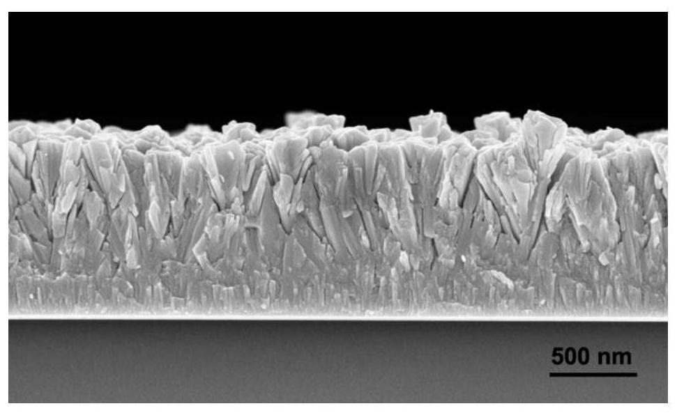
[0044] S2 Send the clean glass wafer substrate into the PbS evaporation reaction chamber until the vacuum degree reaches 5×10 -4After Pa, after raising the substrate temperature to 50 °C, gradually increase the PbS source temperature to the eruption temperature. Then introduce the chlorine gas with a flow rate of 10 sccm, and adjust the vacuum system suction so that the vacuum degree in the reaction chamber is maintained at 2 × 10 -2 Pa. After stabilization, open the growth shutter and start the PbS thin film deposition. After 2 hours, close the baffle, stop the PbS source and the substrate heating power supply, and stop the input of chlorine gas. The film thickness was 1.2 microns. The PbS deposition...
Embodiment 2
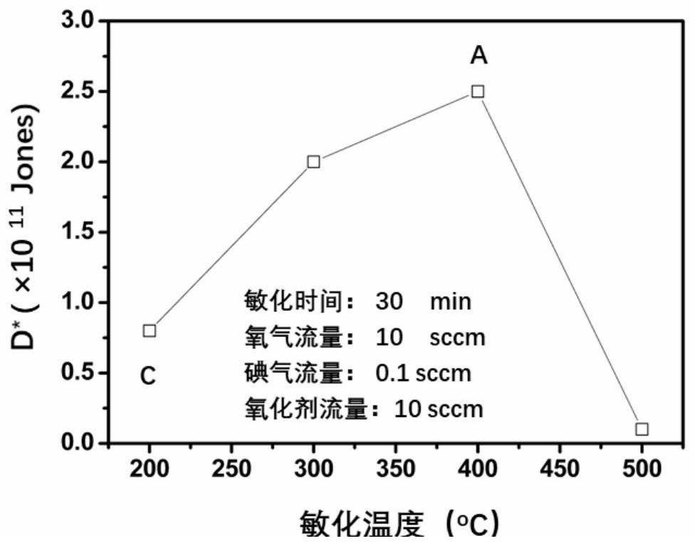
[0047] S1 Place the high-resistance silicon wafer in a high-temperature furnace for high-temperature oxidation thermal cleaning. The thermal cleaning temperature is 600° C., the thermal cleaning time is 3 hours, and the oxygen flow rate is 10 sccm.
[0048] S2 sends the clean Si wafer into the PbS evaporation reaction chamber, and waits until the vacuum degree reaches 5×10 -4 After Pa, after raising the substrate temperature to 50 °C, gradually increase the PbS source temperature to the eruption temperature. Then introduce the chlorine gas with a flow rate of 10 sccm, and adjust the vacuum system suction so that the vacuum degree in the reaction chamber is maintained at 2 × 10 -2 Pa. After stabilization, open the growth shutter and start PbS deposition. After 2h, close the baffle, PbS source and substrate heating power supply, and stop the input of chlorine gas. The film thickness was 1.2 microns. The PbS deposition rate was 0.6 microns / hour.
[0049] S3 Place the PbS th...
Embodiment 3
[0051] S1 Place a 3-inch ordinary glass wafer in acetone, ethanol, and deionized water for 10 minutes, and then place it in concentrated sulfuric acid for 2 hours. Ultrasonic cleaning in deionized water for 10 min, followed by drying to obtain a glass wafer substrate with a clean surface.
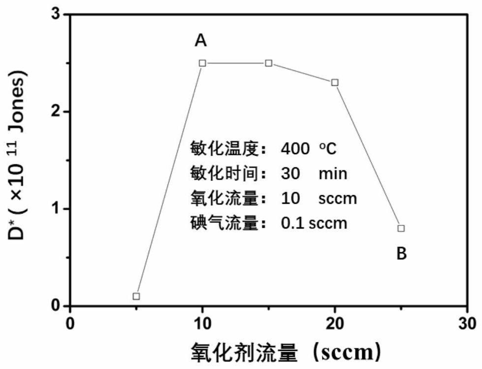
[0052] S2 sends the clean glass substrate into the PbS evaporation reaction chamber until the vacuum degree reaches 2×10 -4 After Pa, after raising the substrate temperature to 50 °C, gradually increase the PbS source temperature to the eruption temperature. Introduce the flow rate subsequently and be the chlorine gas of 25sccm, and adjust the suction of the vacuum system so that the vacuum degree in the reaction chamber is maintained at 5×10 -2 Pa. After stabilization, open the growth shutter and start PbS deposition. After 3 hours, close the baffle, PbS source and substrate heating power supply, and stop the input of oxidant. The film thickness was 1.2 microns. The PbS deposition rat...
PUM
| Property | Measurement | Unit |
|---|---|---|
| thickness | aaaaa | aaaaa |
| thickness | aaaaa | aaaaa |
| thickness | aaaaa | aaaaa |
Abstract
Description
Claims
Application Information
 - R&D Engineer
- R&D Manager
- IP Professional
- Industry Leading Data Capabilities
- Powerful AI technology
- Patent DNA Extraction
Browse by: Latest US Patents, China's latest patents, Technical Efficacy Thesaurus, Application Domain, Technology Topic, Popular Technical Reports.
© 2024 PatSnap. All rights reserved.Legal|Privacy policy|Modern Slavery Act Transparency Statement|Sitemap|About US| Contact US: help@patsnap.com