Image sensor and pixel array circuit thereof

An image sensor and pixel array technology, applied in the field of image sensors, can solve the problems of limiting the swingable range of output voltage signals, the inability to obtain digital pixel values, DC offset, etc., and achieve the effect of increasing the swingable range

Inactive Publication Date: 2020-08-21
GUANGZHOU TYRAFOS SEMICON TECH CO LTD
View PDF6 Cites 0 Cited by
  • Summary
  • Abstract
  • Description
  • Claims
  • Application Information

AI Technical Summary

Problems solved by technology

Dark current will cause the output voltage signal generated by the pixel array circuit to have a DC offset (DC offset)
In the case of a large DC offset, the swing range of the output voltage signal will be greatly limited, so that the readout circuit of the image sensor will experience signal saturation or fail to obtain the correct digital pixel in the process of processing the output voltage signal. value

Method used


Image

  • Image sensor and pixel array circuit thereof
  • Image sensor and pixel array circuit thereof
  • Image sensor and pixel array circuit thereof

Examples


Embodiment Construction

[0037] Reference will now be made in detail to the exemplary embodiments of the present invention, examples of which are illustrated in the accompanying drawings. In addition, wherever possible, elements / components using the same reference numerals in the drawings and embodiments represent the same or similar parts.

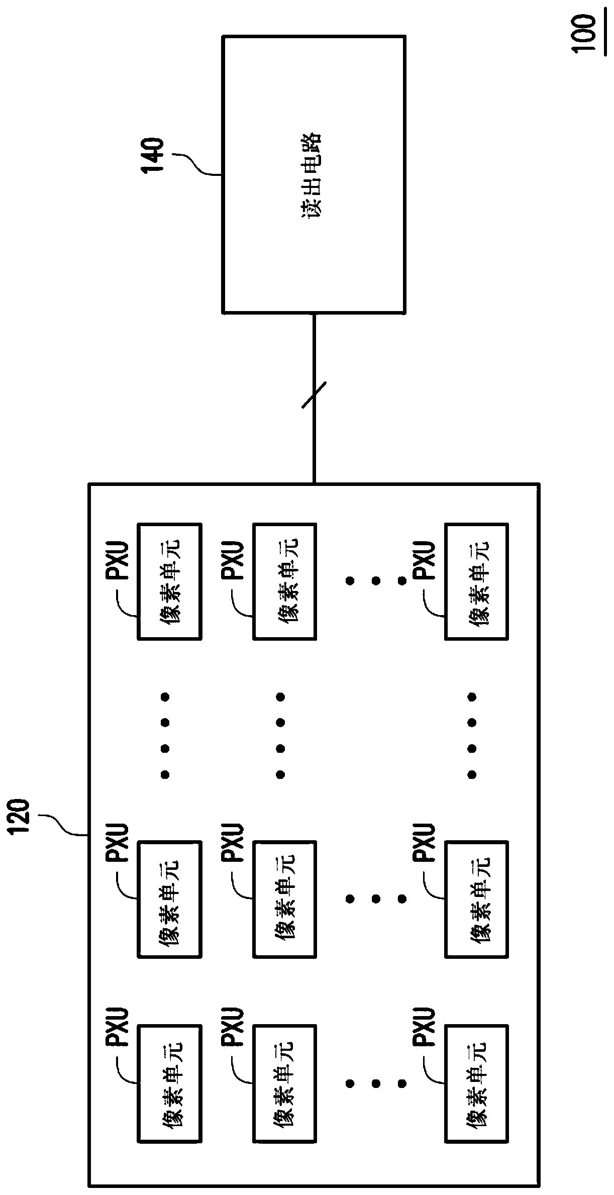
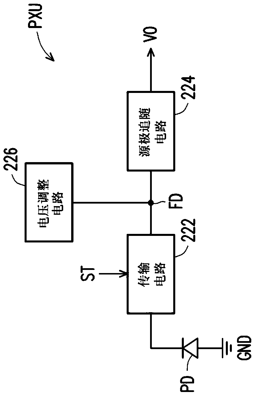
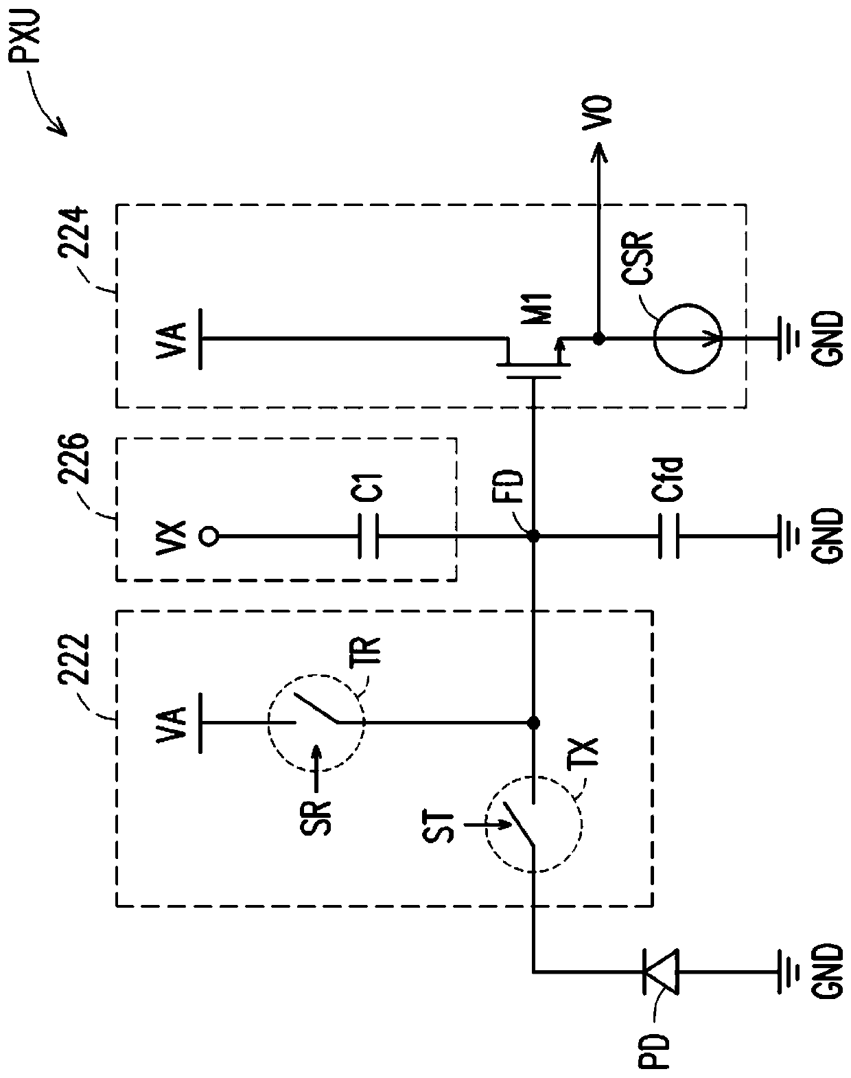
[0038] figure 1 is a schematic circuit block diagram of an image sensor according to an embodiment of the present invention, figure 2 It is a schematic circuit block diagram of a pixel unit according to an embodiment of the present invention. Please merge reference figure 1 and figure 2 , the image sensor 100 may include a pixel array circuit 120 and a readout circuit 140 . The pixel array circuit 120 may include a plurality of pixel units PXU arranged in an array. Each pixel unit PXU may include a photo sensor PD, a transmission circuit 222 , a source follower circuit 224 and a voltage adjustment circuit 226 , but the invention is not limited thereto.

...


PUM


Abstract

The invention provides an image sensor and a pixel array circuit thereof. The image sensor includes a pixel array circuit and a readout circuit. The pixel array circuit comprises a plurality of pixelunits. Each pixel unit comprises an optical sensor, a transmission circuit, a source following circuit and a voltage adjusting circuit, wherein the transmission circuit is coupled between the light sensor and a floating diffusion node, and is controlled by the transmission control signal to control charge transmission between the light sensor and the floating diffusion node; the source following circuit is coupled to the floating diffusion node and is used for converting the voltage of the floating diffusion node into an output voltage signal; the voltage adjusting circuit is coupled to the floating diffusion node and is used for adjusting the DC level of the voltage of the floating diffusion node so as to increase the swingable range of the output voltage signal. The readout circuit is coupled to the source following circuit of each pixel unit to receive the output voltage signal, and processes the output voltage signal to obtain a corresponding digital pixel value.

Description

technical field [0001] The present invention relates to an image sensor, in particular to an image sensor capable of adjusting the DC offset of a floating diffusion node and a pixel array circuit thereof. Background technique [0002] In general, dark current is one of the main noise sources of image sensors. In detail, when the photo-sensing element in the pixel array circuit of the image sensor is not exposed, the current that the photo-sensing element can still generate is the so-called dark current. The dark current will cause the output voltage signal generated by the pixel array circuit to have a DC offset. In the case of a large DC offset, the swing range of the output voltage signal will be greatly limited, so that the readout circuit of the image sensor will experience signal saturation or fail to obtain the correct digital pixel in the process of processing the output voltage signal. value. Contents of the invention [0003] In view of this, the present invent...

Claims


Application Information

Patent Timeline
Patent Type & Authority Applications(China)
IPC IPC(8): H04N5/225H04N5/335H04N5/361
CPCH04N23/54H04N25/00H04N25/63
Inventor 印秉宏王佳祥
Owner GUANGZHOU TYRAFOS SEMICON TECH CO LTD
Why Eureka
Try Eureka