Display panel and display device
A display panel and display area technology, which is applied to identification devices, instruments, semiconductor devices, etc., can solve the problems of display screens with unfavorable narrow borders, increase the width of the borders of the display screen, and reduce the display effect of the display screen, so as to improve the display effect, The effect of improving display quality and reducing light leakage rate
- Summary
- Abstract
- Description
- Claims
- Application Information
AI Technical Summary
Problems solved by technology
Method used
Image
Examples
Embodiment 1
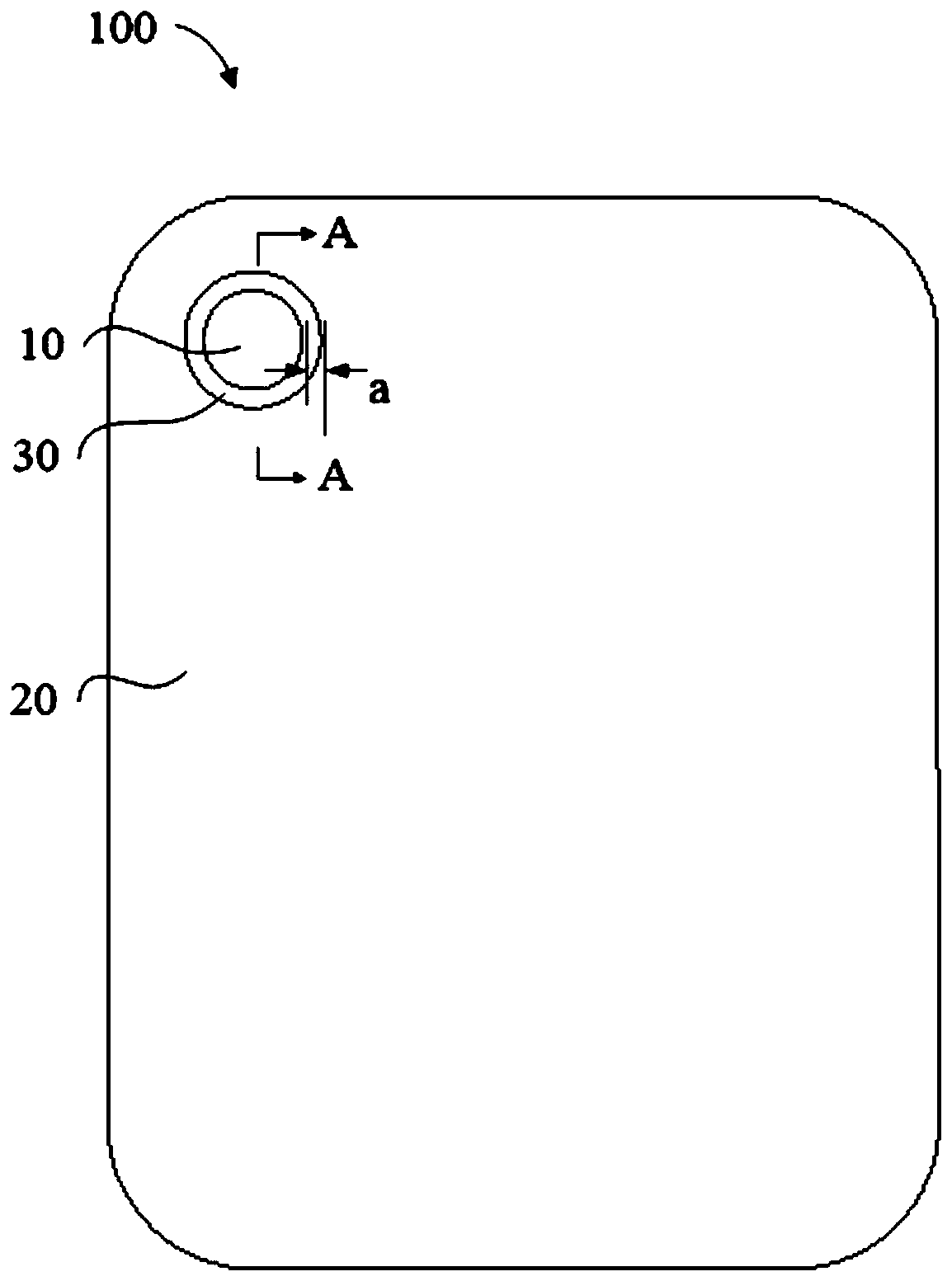
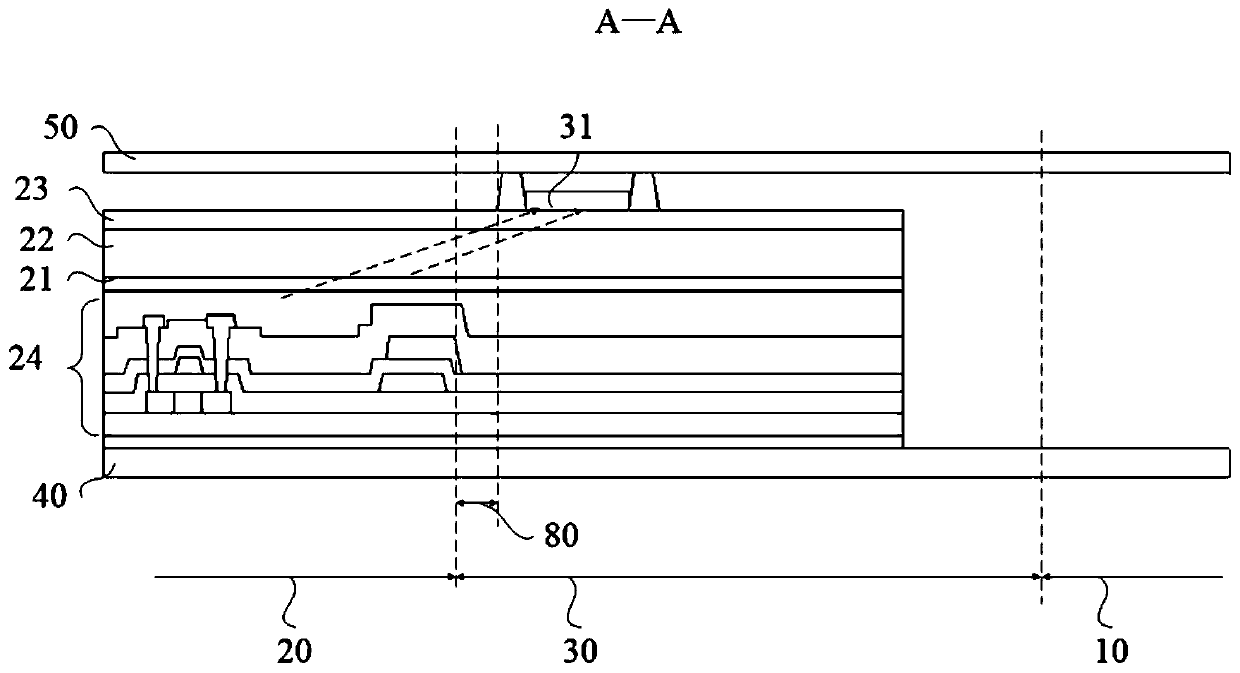
[0058] figure 1 It is a schematic structural diagram of a display panel provided by Embodiment 1 of the present invention. figure 2 Provided for Embodiment 1 of the present invention figure 1 Schematic diagram of the cross-sectional structure of A-A. image 3 It is a schematic structural diagram of the first light-shielding layer of the display panel provided by Embodiment 1 of the present invention. Figure 4 A schematic diagram of the influence of the distance between the light-shielding layer and the light-emitting layer of the display panel on the light-shielding effect provided by Embodiment 1 of the present invention.
[0059] refer to Figure 1 to Figure 4 As shown, the present invention provides a display panel 100 , including a light-transmitting area 10 and a display area 20 at least partially surrounding the light-transmitting area 10 , and a light-shielding area 30 is disposed between the display area 20 and the light-transmitting area 10 .
[0060] An array s...
Embodiment 2
[0081] Figure 5 It is a schematic structural diagram of the second light-shielding layer of the display panel provided by Embodiment 2 of the present invention. refer to Figure 5 As shown, on the basis of the first embodiment above, the second embodiment of the present invention provides a display panel. Compared with the first embodiment, the difference between the second embodiment and the first embodiment is that the position of the light-shielding layer 31 is different. .
[0082] Specifically, the light-shielding layer 31 includes a second light-shielding layer 312 disposed between the insulating barrier layer 60 and the encapsulation layer 50 , and the second light-shielding layer 312 is in contact with the second electrode layer 23 through the insulating barrier layer 60 .
[0083] It should be noted that the second light-shielding layer 312 can be a single-layer light-shielding layer or a composite light-shielding layer. The material for forming the second light-s...
Embodiment 3
[0087] Figure 6 A schematic structural diagram of the first light-shielding layer and the second light-shielding layer of the display panel provided by Embodiment 3 of the present invention. refer to Figure 6 As shown, on the basis of Embodiment 1 or Embodiment 2 above, Embodiment 3 of the present invention provides a display panel. Compared with Embodiment 1 or Embodiment 2, Embodiment 3 differs in that: the light-shielding layer 31 The number and installation position vary.
[0088] Specifically, at least one light-shielding layer 31 includes a first light-shielding layer 311 disposed between the second electrode layer 23 and the insulating barrier layer 60 , and a second light-shielding layer 312 disposed between the insulating barrier layer 60 and the encapsulation layer 50 .
[0089] It should be noted that the area of the effective light-shielding region of the light-emitting layer is increased by the first light-shielding layer 311 to enhance the light-shielding ...
PUM
 Abstract
Description
Claims
Application Information
 - R&D
- Intellectual Property
- Life Sciences
- Materials
- Tech Scout
- Unparalleled Data Quality
- Higher Quality Content
- 60% Fewer Hallucinations
Browse by: Latest US Patents, China's latest patents, Technical Efficacy Thesaurus, Application Domain, Technology Topic, Popular Technical Reports.
© 2025 PatSnap. All rights reserved.Legal|Privacy policy|Modern Slavery Act Transparency Statement|Sitemap|About US| Contact US: help@patsnap.com


