Eureka AIR delivers breakthrough ideas for toughest innovation challenges, trusted by R&D personnel around the world.

Image compensation method and image processing circuit

An image compensation and image processing technology, applied in the field of image processing

Pending Publication Date: 2020-07-07
NOVATEK MICROELECTRONICS CORP
View PDF4 Cites 2 Cited by
  • Summary
  • Abstract
  • Description
  • Claims
  • Application Information

AI Technical Summary

Problems solved by technology

That is, the user may see color fringes of unexpected colors at the edges of the color blocks displayed in the image frame

Method used


Image

  • Image compensation method and image processing circuit
  • Image compensation method and image processing circuit
  • Image compensation method and image processing circuit

Examples


Embodiment Construction

[0022] Reference will now be made in detail to the exemplary embodiments of the present invention, examples of which are illustrated in the accompanying drawings. Wherever possible, the same reference numbers will be used in the drawings and description to refer to the same or like parts.

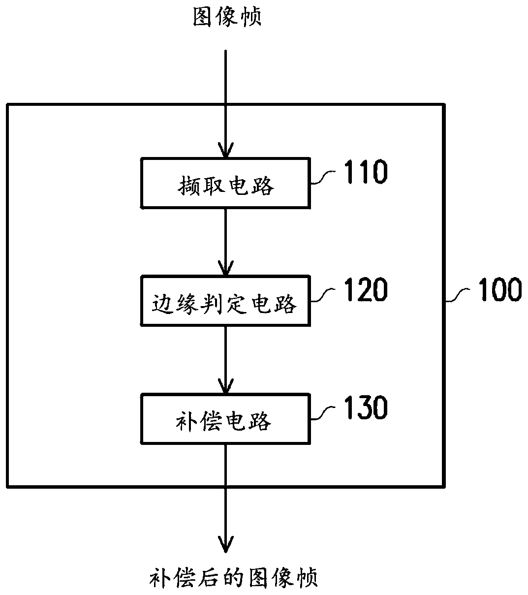
[0023] see figure 1 , figure 1 It is a schematic diagram of a circuit block of an image processing circuit 100 according to an embodiment of the present invention. According to application requirements, figure 1 The illustrated image processing circuit 100 may be applied to any type of display. For example, the display may include a liquid crystal display panel, an organic electro-luminescence display panel, a plasma display panel, an electronic paper display panel ( electronic paper panel), electro wetting display panel (electro wetting display panel) or other types of display panels.

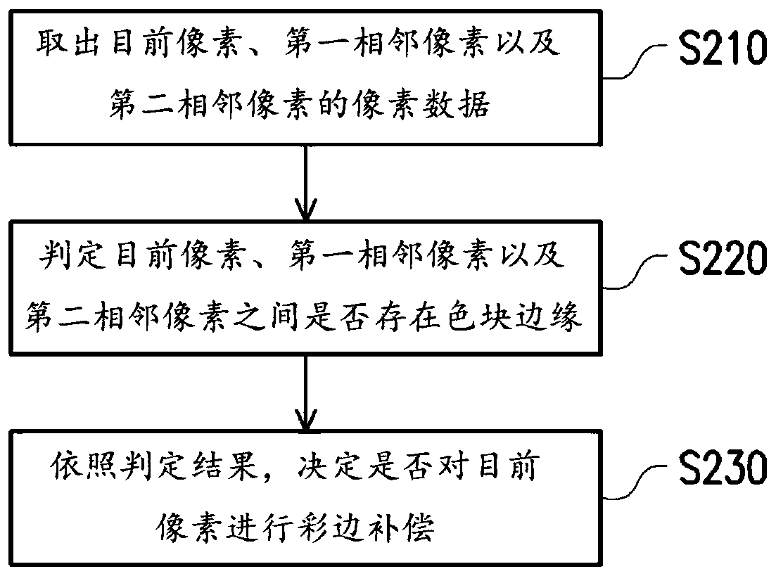
[0024] figure 2 It is a schematic flowchart of an image compensation method according to an embod...


PUM


Abstract

The invention provides an image compensation method suitable to a display. First, an image processing circuit obtains pixel data related to a current pixel, a first and a second adjacent pixels from an image frame. The first and the second adjacent pixels are respectively located at two opposite sides of the current pixel. Then, the image processing circuit determines whether a color block edge exists between the current pixel, the first adjacent pixel and the second adjacent pixel according to the pixel data related to the current pixel, the first adjacent pixel and the second adjacent pixel.The image processing circuit performs first color edge compensation on the pixel data related to the current pixel when determining that the color block edge exists between the current pixel and thefirst adjacent pixel and no color block edge exists between the current pixel and the second adjacent pixel. An image processing circuit is further provided.

Description

technical field [0001] The invention relates to an image processing technology, in particular to an image compensation method and an image processing circuit. Background technique [0002] In a display panel in which the ratio of light emitted by subpixels (Subpixels) is controlled to form an image through color mixing, the arrangement (Arrangement) of subpixels of each pixel has a certain degree of non-uniformity. For example, whether it is true color (truecolor) sub-pixel arrangement or sub-pixel rendering (Subpixel Rendering, SPR) sub-pixel arrangement, these arrangements all have a certain degree of non-uniformity. Due to the non-uniform arrangement of sub-pixels, color fringing may occur on the edges of objects in the image frame. The color fringing phenomenon comes from the fact that each edge of a pixel does not have three primary color sub-pixels, so the edge of a color block (object) after human visual integration may appear in an unexpected color. That is, the us...

Claims


Application Information

Patent Timeline
IPC IPC(8): G09G3/20
CPCG09G3/2003G06T2207/10024G09G2320/0242G09G2360/16G06T5/00G09G5/02G09G2320/029G06T5/73
Inventor 简又仪
Owner NOVATEK MICROELECTRONICS CORP
Why Eureka
Eureka Blog
Learn More