Circuit board via hole impedance optimization method and circuit board

An optimization method and circuit board technology, applied in printed circuit, printed circuit manufacturing, computer design circuit, etc., can solve problems such as high process cost, affecting the integrity of transmission signals, and inability to completely remove via stubs

Active Publication Date: 2020-06-26
SUZHOU LANGCHAO INTELLIGENT TECH CO LTD
View PDF5 Cites 6 Cited by
  • Summary
  • Abstract
  • Description
  • Claims
  • Application Information

AI Technical Summary

Problems solved by technology

However, the back-drilling process cannot completely remove the stumps of the vias, and there are still stumps within about 12mil, which affect the integrity of the transmission signal; although the deep micro-hole technology can completely remove the stumps of the vias, the process cost is relatively high

Method used


Image

  • Circuit board via hole impedance optimization method and circuit board
  • Circuit board via hole impedance optimization method and circuit board
  • Circuit board via hole impedance optimization method and circuit board

Examples


Embodiment Construction

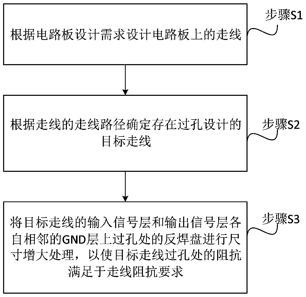
[0037] The core of the present invention is to provide a circuit board via impedance optimization method and circuit board, by changing the shape of the anti-pad at the wiring via to optimize the impedance continuity at the via, so as not to increase the process cost. It satisfies the integrity requirements of the transmission signal; moreover, this application changes the shape of the anti-pad at the via on the adjacent GND layer of the input signal layer and the output signal layer of the trace, while optimizing the impedance at the via Will not affect the impedance of the trace.

[0038] In order to make the objectives, technical solutions, and advantages of the embodiments of the present invention clearer, the technical solutions in the embodiments of the present invention will be described clearly and completely in conjunction with the accompanying drawings in the embodiments of the present invention. Obviously, the described embodiments It is a part of the embodiments of th...


PUM


Abstract

The invention discloses an impedance optimization method of a circuit board via hole. The impedance optimization method comprises the steps: designing wiring on a circuit board according to a circuitboard design requirement; determining a target wire with via hole design according to the routing path of the wire; and carrying out size increase processing on the anti-bonding pads at the via holesin the GND layers adjacent to the input signal layer and the output signal layer of the target wire so as to enable the impedance at the via holes of the target wire to meet the impedance requirementof the wire. Therefore, the impedance continuity at the via hole is optimized by changing the shape of the anti-bonding pad at the wiring via hole, so the integrity requirement of a transmission signal is met under the condition that the process cost is not increased; moreover, the shapes of the anti-pads at the via holes in the GND layers adjacent to the input signal layer and the output signal layer of the wire are changed, so the impedance of the wire is not influenced while the impedance at the via holes is optimized. The invention also discloses a circuit board which has the same beneficial effects as the impedance optimization method.

Description

Technical field [0001] The invention relates to the field of circuit board design, in particular to a method for optimizing the impedance of a circuit board via hole and a circuit board. Background technique [0002] According to transmission line theory, the point where the impedance is discontinuous will affect the integrity of the transmission signal. In the circuit board wiring design, there are stubs at the wiring vias, which causes the impedance at the vias to be capacitive, that is, the impedance at the vias is low, which causes the impedance at the vias to be discontinuous, restricting transmission For signal integrity, especially for traces with higher signal transmission rates, the continuity of via impedance is more prominent. In the prior art, the back-drilling or deep micro-hole process is usually used to remove the via residual piles to optimize the impedance at the via. However, the back-drilling process cannot completely remove the via stubs, and there are still...

Claims


Application Information

Patent Timeline
Patent Type & Authority Applications(China)
IPC IPC(8): H05K3/42H05K3/00
CPCH05K3/0005H05K3/42
Inventor 田民政
Owner SUZHOU LANGCHAO INTELLIGENT TECH CO LTD
Why Eureka
Try Eureka