Epitaxial growth device and manufacturing method thereof
An epitaxial growth and structure control technology, applied in the semiconductor field, can solve the problems of fast chemical reaction rate, uneven film thickness, thick silicon film, etc., to reduce the temperature, improve the uniformity of film formation, and solve the effects of uneven heating
- Summary
- Abstract
- Description
- Claims
- Application Information
AI Technical Summary
Problems solved by technology
Method used
Image

Examples
Embodiment 1
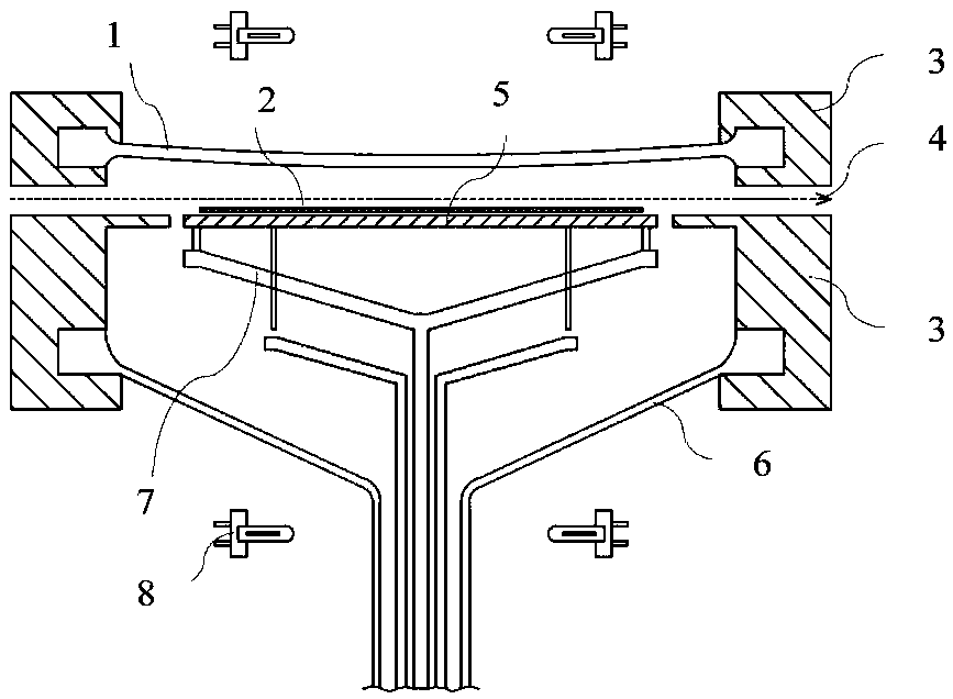
[0066] Such as figure 2 As shown, the epitaxial growth device of the present embodiment comprises an upper quartz bell jar 1 (i.e. the first quartz bell jar) and a lower quartz bell jar 6 (i.e. the second quartz bell jar), the upper quartz bell jar 1 is circular, and the lower quartz bell jar 6 is in the shape of Funnel-shaped, the upper quartz bell jar 1 and the lower quartz bell jar 6 form a reaction chamber through the installation part 3. The reaction chamber includes an air inlet and an exhaust port. The reaction gas enters through the air inlet and deposits an epitaxial film through a high-temperature chemical reaction. , the exhaust gas produced is discharged through the exhaust port, where 4 is the airflow direction. A base 5 for placing a silicon wafer 2 is arranged inside the reaction chamber, and the base 5 is fixed and kept in a horizontal state by a base support frame 7 . During the chemical gas phase reaction, the base support frame 7 drives the base 5 to rotat...
Embodiment 2
[0075] Such as Figure 5 As shown, the epitaxial growth device of the present embodiment comprises an upper quartz bell jar 1 (i.e. the first quartz bell jar) and a lower quartz bell jar 6 (i.e. the second quartz bell jar), the upper quartz bell jar 1 is circular, and the lower quartz bell jar 6 is in the shape of Funnel-shaped, the upper quartz bell jar 1 and the lower quartz bell jar 6 form a reaction chamber through the installation part 3. The reaction chamber includes an air inlet and an exhaust port. The reaction gas enters through the air inlet and deposits an epitaxial film through a high-temperature chemical reaction. , the exhaust gas produced is discharged through the exhaust port, where 4 is the airflow direction. A base 5 for placing a silicon wafer 2 is arranged inside the reaction chamber, and the base 5 is fixed and kept in a horizontal state by a base support frame 7 . During the chemical gas phase reaction, the base support frame 7 drives the base 5 to rotat...
Embodiment 3
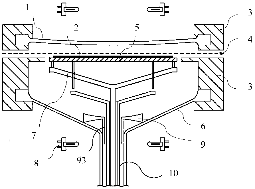
[0082] Such as Figure 8 As shown, the epitaxial growth device of the present embodiment comprises an upper quartz bell jar 1 (i.e. the first quartz bell jar) and a lower quartz bell jar 6 (i.e. the second quartz bell jar), the upper quartz bell jar 1 is circular, and the lower quartz bell jar 6 is in the shape of Funnel-shaped, the upper quartz bell jar 1 and the lower quartz bell jar 6 form a reaction chamber through the installation part 3. The reaction chamber includes an air inlet and an exhaust port. The reaction gas enters through the air inlet and deposits an epitaxial film through a high-temperature chemical reaction. , the exhaust gas produced is discharged through the exhaust port, where 4 is the airflow direction. A base 5 for placing a silicon wafer 2 is arranged inside the reaction chamber, and the base 5 is fixed and kept in a horizontal state by a base support frame 7 . During the chemical gas phase reaction, the base support frame 7 drives the base 5 to rotat...
PUM
 Abstract
Description
Claims
Application Information
 - R&D
- Intellectual Property
- Life Sciences
- Materials
- Tech Scout
- Unparalleled Data Quality
- Higher Quality Content
- 60% Fewer Hallucinations
Browse by: Latest US Patents, China's latest patents, Technical Efficacy Thesaurus, Application Domain, Technology Topic, Popular Technical Reports.
© 2025 PatSnap. All rights reserved.Legal|Privacy policy|Modern Slavery Act Transparency Statement|Sitemap|About US| Contact US: help@patsnap.com