
Method for forming SiO2 waveguide based on wafer bonding to realize speckle conversion and speckle converter

A wafer bonding and waveguide technology, applied in the direction of optical waveguide light guide, light guide, instrument, etc., can solve the problem of waveguide thickness limitation, achieve the effects of reducing coupling accuracy requirements, improving coupling efficiency, and process compatibility

Active Publication Date: 2020-06-05
UNITED MICROELECTRONICS CENT CO LTD
View PDF7 Cites 2 Cited by
  • Summary
  • Abstract
  • Description
  • Claims
  • Application Information

AI Technical Summary

Problems solved by technology

[0004] Aiming at the deficiencies existing in the prior art, the present invention provides a method capable of solving SiO 2 Waveguide Thickness Constraints, Wafer Bonding Formation of SiO for Improving Coupling Efficiency 2 The Method of Waveguide Realizing Mode Spot Conversion

Method used


Image

  • Method for forming SiO2 waveguide based on wafer bonding to realize speckle conversion and speckle converter
  • Method for forming SiO2 waveguide based on wafer bonding to realize speckle conversion and speckle converter
  • Method for forming SiO2 waveguide based on wafer bonding to realize speckle conversion and speckle converter

Examples


Embodiment Construction

[0030] In order to make the technical means, creative features, goals and effects of the invention easy to understand, the present invention will be further elaborated below in conjunction with specific illustrations.

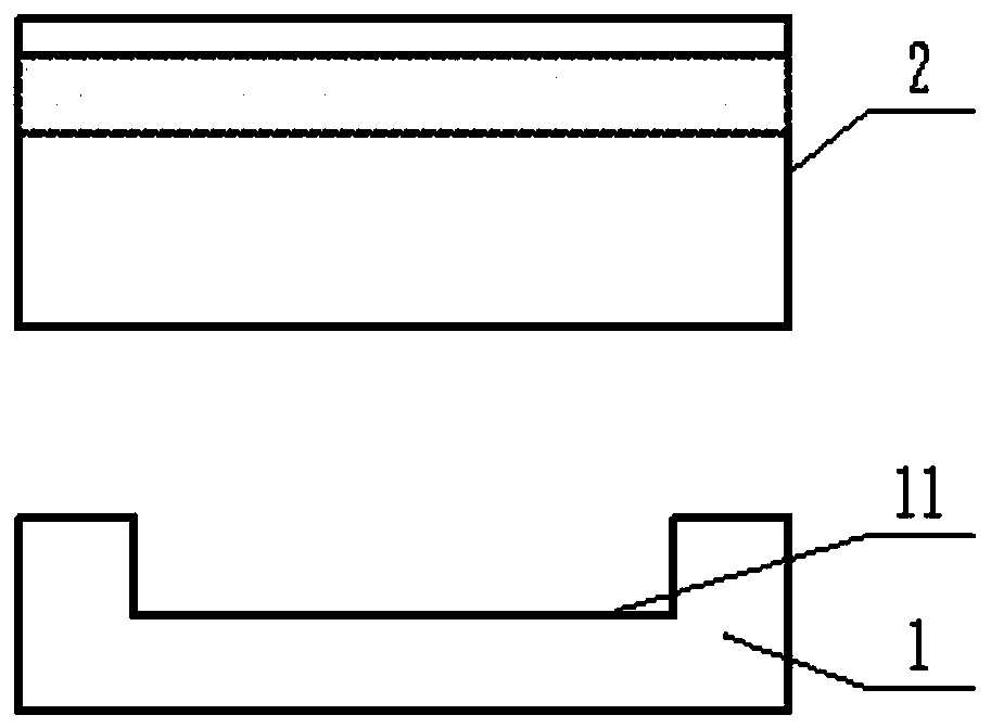
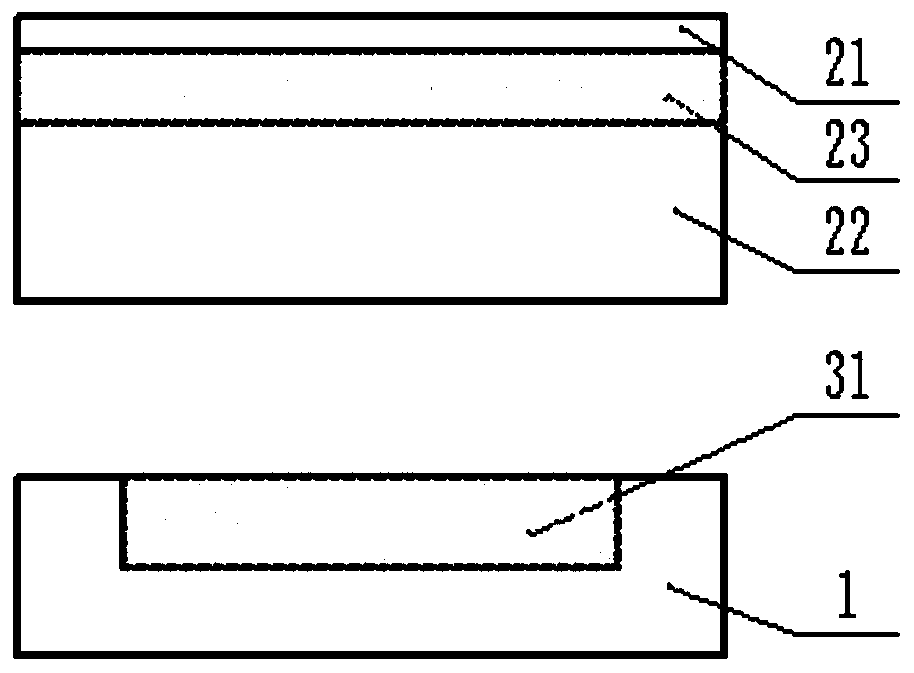
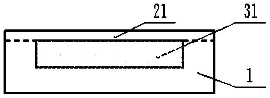
[0031] Formation of SiO based on wafer bonding 2 The method of waveguide to achieve mode spot conversion, such as Figure 1-8 shown (the shaded part is SiO 2 ), including the following steps:

[0032] S1: Prepare a silicon substrate 1 and an SOI wafer 2, and etch a groove 11 on the silicon substrate 1 at a position corresponding to the end-face coupling waveguide, such as figure 1 shown;

[0033] S2: growing SiO in the groove 11 2 To fill the groove 11, and perform chemical mechanical polishing to ensure that the wafer is flat and form the first SiO 2 waveguide layer 31, to complete the preparation of the substrate silicon wafer, such as figure 2 shown;

[0034] S3: Clean the surface of the SOI wafer 2 to ensure that the surface of the SOI wafer 2 is cl...


PUM


Abstract

The invention discloses a method for forming SiO2 waveguide based on wafer bonding to realize speckle conversion and a speckle converter, and the method comprises the steps: preparing a silicon substrate and an SOI wafer, and manufacturing a groove in the silicon substrate; manufacturing a first SiO2 waveguide layer to fill the groove; bonding the top silicon of the SOI wafer to the surface of thesilicon substrate, and removing the substrate silicon layer and the buried oxide layer of the SOI wafer; etching the top silicon, and forming a silicon waveguide on the first SiO2 waveguide layer; manufacturing a second SiO2 waveguide layer on the silicon waveguide and the first SiO2 waveguide layer; and etching the first SiO2 waveguide layer and the second SiO2 waveguide layer to the bottom of the groove to form the SiO2 waveguide. The problem that the thickness of the SiO2 waveguide is limited can be solved, the coupling efficiency can be improved, and the method is compatible with the CMOSprocess.

Description

technical field [0001] The invention belongs to the field of silicon photonics technology, in particular to the formation of SiO based on wafer bonding 2 A method for realizing mode speckle conversion by a waveguide and a mode speckle converter. Background technique [0002] The mode spot conversion technology of the end-coupled waveguide in the silicon photonics chip has always been the core technical difficulty of the commercialization of the silicon photonics chip. The diameter of the mode spot size of the silicon waveguide is around 0.5um, and the mode spot size of the single-mode fiber coupled with it is about 10um , the huge mode mismatch causes a large end-face coupling loss. [0003] In the prior art, the mode spot size of the silicon optical waveguide can be extended to about 3um through the Inverse Taper structure, but due to the substrate SiO 2 Due to the limitation of the thickness of the buried oxide layer (Box) and the upper cladding layer (Cladding), it is d...

Claims


Application Information

Patent Timeline
Patent Type & Authority Applications(China)
IPC IPC(8): G02B6/14G02B6/13G02B6/136G02B6/122G02B6/12
CPCG02B6/14G02B6/13G02B6/136G02B6/1228G02B6/12G02B2006/12197G02B2006/12176G02B2006/12152G02B2006/12038
Inventor 胡志朋吴月邵斯竹肖志雄朱兴国冯俊波郭进
Owner UNITED MICROELECTRONICS CENT CO LTD
Learn More