Display substrate, manufacturing method thereof, display panel and display device

A technology for display substrates and manufacturing methods, applied in the field of display panels and display devices, capable of solving problems such as touch failure, poor cathode partition effect, and abnormal display

Inactive Publication Date: 2020-05-19
BOE TECH GRP CO LTD +1
View PDF5 Cites 7 Cited by
  • Summary
  • Abstract
  • Description
  • Claims
  • Application Information

AI Technical Summary

Problems solved by technology

This cathode isolation scheme usually cannot effectively isolate the cathode, such as figure 2 As shown in the middle ellipse area, the side of the isolation layer 103 is covered with a cathode 104, which will lead to abnormal display or touch failure
Especially when the cathode is made by the sputtering coating (Sputter) process, because the diffusion effect of the sputtering coating process is better, the isolation effect of the cathode is worse
In addition, cracks are prone to occur during the process of cutting the mother board to form multiple display substrates
Once the cracks caused by cutting or other reasons spread to the display area, it will affect the display and touch performance of the product

Method used


Image

  • Display substrate, manufacturing method thereof, display panel and display device
  • Display substrate, manufacturing method thereof, display panel and display device
  • Display substrate, manufacturing method thereof, display panel and display device

Examples


Embodiment Construction

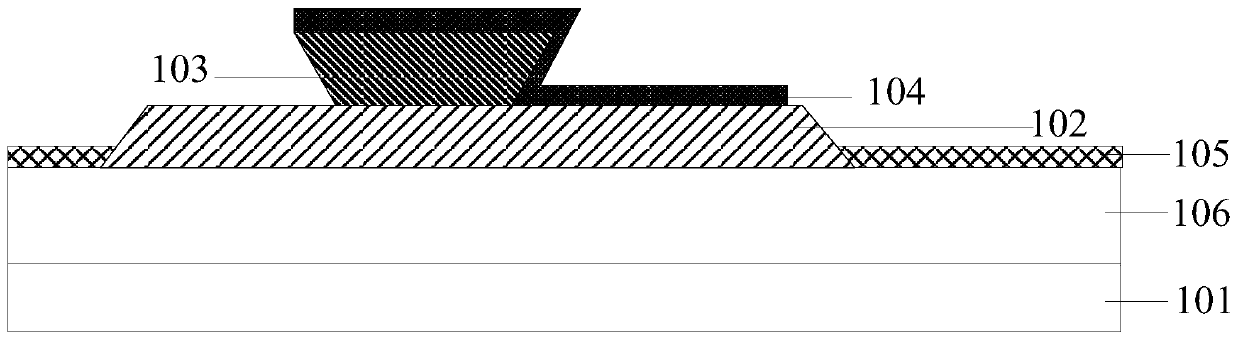
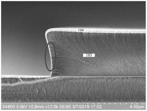
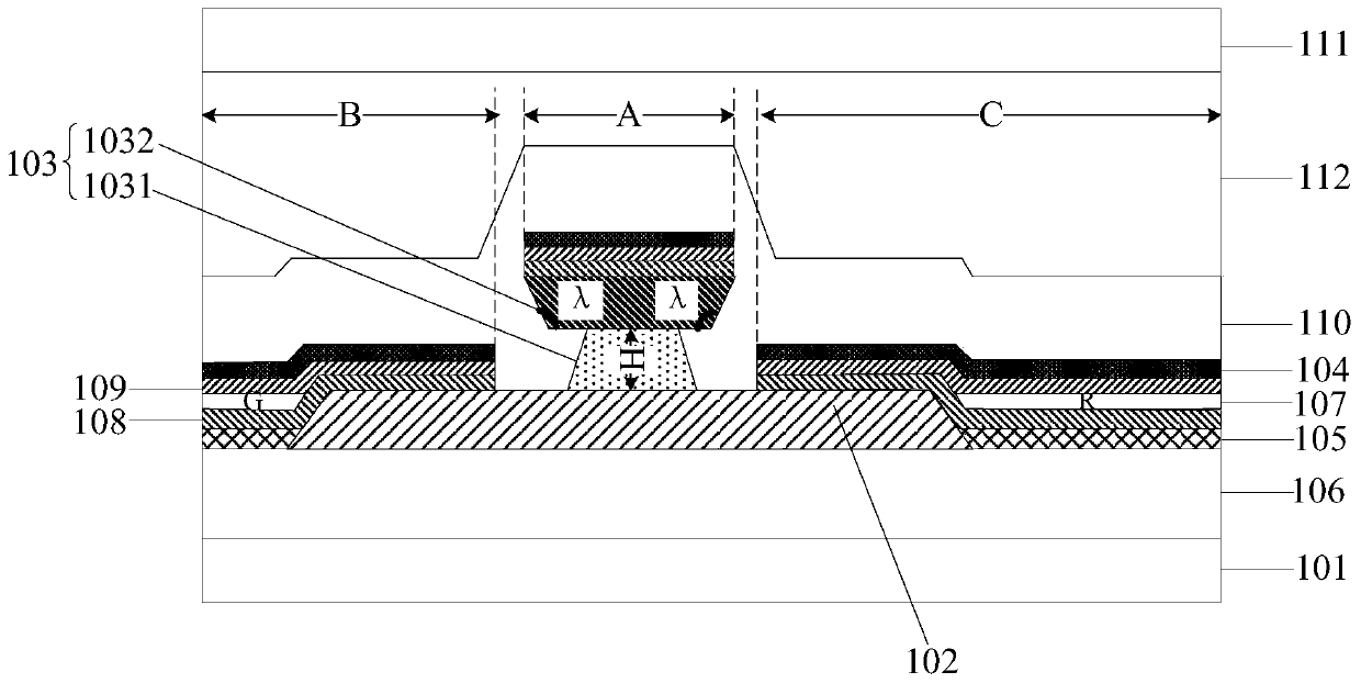
[0076] In order to make the purpose, technical solutions and advantages of the embodiments of the present invention more clear, the following will clearly and completely describe the technical solutions of the embodiments of the present invention in conjunction with the drawings of the embodiments of the present invention. The thickness and shape of each film layer in the drawings do not reflect the real scale, and the purpose is only to illustrate the content of the present invention. Apparently, the described embodiments are some, not all, embodiments of the present invention. Based on the described embodiments of the present invention, all other embodiments obtained by persons of ordinary skill in the art without creative efforts shall fall within the protection scope of the present invention.

[0077] Unless otherwise defined, the technical terms or scientific terms used herein shall have the usual meanings understood by those skilled in the art to which the present invent...


PUM


Abstract

The invention discloses a display substrate, a manufacturing method thereof, a display panel and a display device. Through arrangement of a first isolation part and a second isolation part, a first isolated part is disconnected with at least one of a second isolated part and a third isolated part, so that when the isolated layer is a cathode multiplexed as a self-capacitance electrode, the cathodeisolation effect can be enhanced; when the isolated layer is the inorganic thin film packaging layer contained in the frame area, cracks generated by cutting or other reasons can be prevented from expanding to the display area; and therefore, the display quality and the touch effect are improved.

Description

technical field [0001] The invention relates to the field of display technology, in particular to a display substrate, a manufacturing method thereof, a display panel, and a display device. Background technique [0002] Organic electroluminescent display (OLED) products have the advantages of fast response speed, thin thickness, and high contrast, and have gradually begun to encroach on the market of liquid crystal display (LCD) products, especially their bendable and flexible features. Become the preferred technology for flexible display devices. However, in OLED products with a touch function, it is necessary to separate the cathodes of different pixels or different regions so as to be reused as self-capacitance electrodes. [0003] Such as figure 1 Shown is a schematic diagram of a cathode isolation scheme in the prior art. Specifically, it includes: a base substrate 101, a pixel definition layer 102, an isolation layer 103, a cathode 104, an anode 105, and a transisto...

Claims


Application Information

Patent Timeline
Patent Type & Authority Applications(China)
IPC IPC(8): H01L27/32H01L51/56
CPCH10K59/40H10K59/122H10K71/00H10K50/8445G06F3/0412G06F3/044H10K59/1201
Inventor 徐传祥舒适姚琪袁广才黄海涛于勇岳阳孙中元
Owner BOE TECH GRP CO LTD
Why Eureka
Try Eureka