Display panel and preparation method thereof

A technology for display panels and array substrates, applied to instruments, electrical components, diodes, etc., can solve the problems of light damage, affecting the performance of display panels, and high manufacturing costs

Inactive Publication Date: 2020-04-24
WUHAN CHINA STAR OPTOELECTRONICS SEMICON DISPLAY TECH CO LTD
View PDF9 Cites 4 Cited by
  • Summary
  • Abstract
  • Description
  • Claims
  • Application Information

AI Technical Summary

Problems solved by technology

[0002] At present, in the preparation of display panels, in the preparation process of the light-emitting layer of the display panel, multi-channel precision mask process and high-precision alignment process of inductively coupled devices are required, which makes the process complicated, low yield rate, and high production cost. , and a polarizer needs to be pasted, resulting in light damage, which in turn affects the performance of the display panel, and the manufacturing cost is high

Method used


Image

  • Display panel and preparation method thereof
  • Display panel and preparation method thereof
  • Display panel and preparation method thereof

Examples


Embodiment Construction

[0032] The following will clearly and completely describe the technical solution in the application with reference to the accompanying drawings in the implementation manner of the application. Apparently, the described implementations are only some of the implementations of this application, not all of them. Based on the implementation manners in this application, all other implementation manners obtained by those skilled in the art without creative efforts shall fall within the scope of protection of this application.

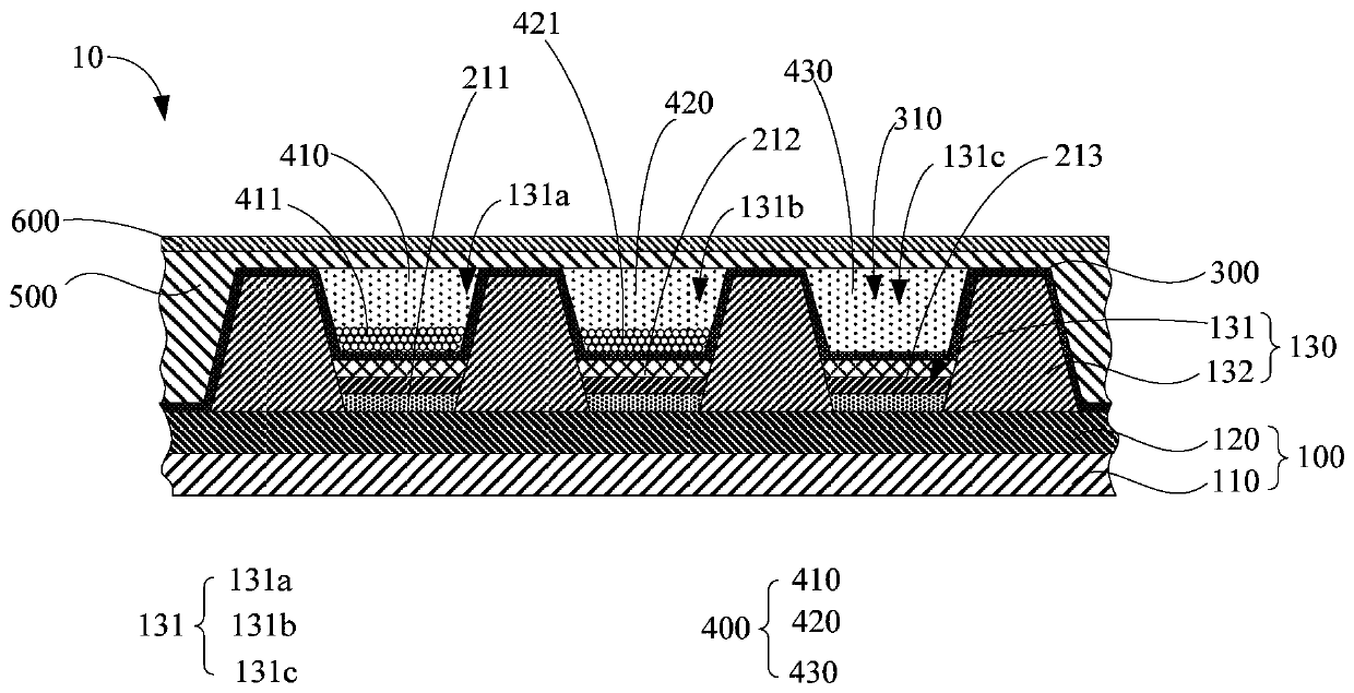
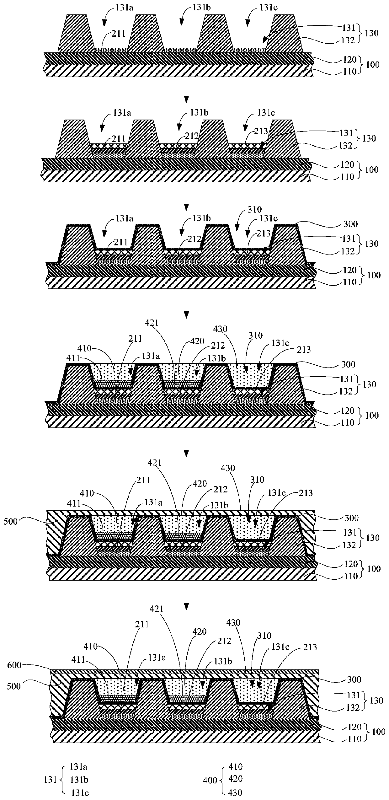
[0033] see figure 1 , figure 1 A cross-sectional view of the display panel provided for this application. The display panel 10 includes an array substrate 100 , a light emitting layer 200 , a first barrier layer 300 , a color filter layer 500 , a flat layer 600 and a second barrier layer 700 .

[0034] The array substrate 100 includes a thin film transistor layer 120 and a glass substrate 110 . The TFT layer 120 is disposed on the glass substrate 110 . A ...


PUM


Abstract

The invention provides a display panel and a preparation method thereof. The display panel comprises an array substrate, a light-emitting layer, a first barrier layer, a color film layer, a flat layerand a second barrier layer. The array substrate is provided with a pixel definition layer. The pixel definition layer comprises a plurality of pixel definition areas and retaining walls arranged among the pixel definition areas. The light-emitting layer is arranged in the plurality of pixel definition areas. The first barrier layer covers the array substrate, the pixel definition layer and the light-emitting layer. A plurality of grooves are formed in the first barrier layer. The color film layer is arranged in the grooves. The flat layer covers the first barrier layer and the color film layer. The second barrier layer is arranged on the flat layer. According to the display panel provided by the invention, the first barrier layer is arranged on the light-emitting layer, so that the performance of the display panel is improved.

Description

technical field [0001] The present application relates to the field of display panels, in particular to a display panel and a preparation method thereof. Background technique [0002] At present, in the preparation of display panels, in the preparation process of the light-emitting layer of the display panel, multi-channel precision mask process and high-precision alignment process of inductively coupled devices are required, which makes the process complicated, low yield rate, and high production cost. , and a polarizer needs to be pasted, resulting in light damage, thereby affecting the performance of the display panel, and the manufacturing cost is high. Contents of the invention [0003] The present application provides a display panel and a manufacturing method thereof, so as to improve the performance of the display panel, improve the manufacturing efficiency of the display panel, and reduce the production cost. [0004] The application provides a display panel, inc...

Claims


Application Information

Patent Timeline
Patent Type & Authority Applications(China)
IPC IPC(8): H01L27/32H01L27/15G09F9/33
CPCH01L27/156G09F9/33H10K59/38H10K59/122H10K59/1201H10K50/115H10K71/00
Inventor 夏存军李们在
Owner WUHAN CHINA STAR OPTOELECTRONICS SEMICON DISPLAY TECH CO LTD
Why Eureka
Try Eureka